MPC8343VRAGDB Freescale Semiconductor, MPC8343VRAGDB Datasheet - Page 59
MPC8343VRAGDB
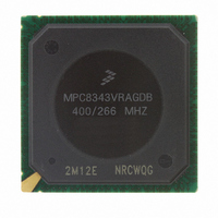
Manufacturer Part Number
MPC8343VRAGDB
Description
IC MPU POWERQUICC II 620-PBGA
Manufacturer
Freescale Semiconductor
Series
PowerQUICC II PROr
Datasheet
1.MPC8343VRAGDB.pdf
(79 pages)
Specifications of MPC8343VRAGDB
Processor Type
MPC83xx PowerQUICC II Pro 32-Bit
Speed
400MHz
Voltage
1.2V
Mounting Type
Surface Mount
Package / Case
620-PBGA
Processor Series
MPC8xxx
Core
e300
Data Bus Width
32 bit
Development Tools By Supplier
MPC8349E-MITXE
Maximum Clock Frequency
400 MHz
Maximum Operating Temperature
+ 105 C
Mounting Style
SMD/SMT
I/o Voltage
1.8 V, 2.5 V, 3.3 V
Minimum Operating Temperature
0 C
Core Size
32 Bit
Program Memory Size
64KB
Cpu Speed
400MHz
Embedded Interface Type
I2C, SPI, USB, UART
Digital Ic Case Style
BGA
No. Of Pins
620
Rohs Compliant
Yes
Family Name
MPC83xx
Device Core
PowerQUICC II Pro
Device Core Size
32b
Frequency (max)
400MHz
Instruction Set Architecture
RISC
Supply Voltage 1 (typ)
1.2V
Operating Supply Voltage (max)
1.26V
Operating Supply Voltage (min)
1.14V
Operating Temp Range
0C to 105C
Operating Temperature Classification
Commercial
Mounting
Surface Mount
Pin Count
620
Package Type
BGA
For Use With
CWH-PPC-8343N-VX - KIT EVAL SYSTEM QUICCSTART 8248CWH-PPC-8343N-VE - EVALUATION SYSTEM QUICC MPC8343E
Lead Free Status / RoHS Status
Lead free / RoHS Compliant
Features
-
Lead Free Status / Rohs Status
Lead free / RoHS Compliant
Available stocks
Company
Part Number
Manufacturer
Quantity
Price
Company:

Part Number:
MPC8343VRAGDB
Manufacturer:
Freescale Semiconductor
Quantity:
135
Company:
Part Number:
MPC8343VRAGDB
Manufacturer:
Freescale Semiconductor
Quantity:
10 000
Part Number:
MPC8343VRAGDB
Manufacturer:
FREESCALE
Quantity:
20 000


19 Clocking
Figure 36
The primary clock source can be one of two inputs, CLKIN or PCI_CLK, depending on whether the device
is configured in PCI host or PCI agent mode. When the MPC8343EA is configured as a PCI host device,
CLKIN is its primary input clock. CLKIN feeds the PCI clock divider (÷2) and the multiplexors for
PCI_SYNC_OUT and PCI_CLK_OUT. The CFG_CLKIN_DIV configuration input selects whether
CLKIN or CLKIN/2 is driven out on the PCI_SYNC_OUT signal. The OCCR[PCICDn] parameters select
whether CLKIN or CLKIN/2 is driven out on the PCI_CLK_OUTn signals.
PCI_SYNC_OUT is connected externally to PCI_SYNC_IN to allow the internal clock subsystem to
synchronize to the system PCI clocks. PCI_SYNC_OUT must be connected properly to PCI_SYNC_IN,
with equal delay to all PCI agent devices in the system, to allow the MPC8343EA to function. When the
device is configured as a PCI agent device, PCI_CLK is the primary input clock and the CLKIN signal
should be tied to GND.
Freescale Semiconductor
CFG_CLKIN_DIV
shows the internal distribution of the clocks.
MPC8343EA PowerQUICC II Pro Integrated Host Processor Hardware Specifications, Rev. 10
CLKIN
MPC8343EA
System PLL
Figure 36. MPC8343EA Clock Subsystem
e300 Core
PCI Clock
csb_clk
Clock
Divider
Unit
csb_clk to Rest
of the Device
ddr_clk
lbiu_clk
Core PLL
To Local Bus
Controller
Controller
Memory
To DDR
Memory
Clock
LBIU
DDR
/n
DLL
Div
/2
core_clk
4
4
5
LCLK[0:2]
LSYNC_OUT
LSYNC_IN
MCK[0:3]
MCK[0:3]
PCI_CLK_OUT[0:4]
PCI_CLK/
PCI_SYNC_IN
PCI_SYNC_OUT
DDR
Memory
Device
Local Bus
Memory
Device
Clocking
59
Related parts for MPC8343VRAGDB
Image
Part Number
Description
Manufacturer
Datasheet
Request
R

Part Number:
Description:
Manufacturer:
Freescale Semiconductor, Inc
Datasheet:
Part Number:
Description:
Manufacturer:
Freescale Semiconductor, Inc
Datasheet:
Part Number:
Description:
Manufacturer:
Freescale Semiconductor, Inc
Datasheet:
Part Number:
Description:
Manufacturer:
Freescale Semiconductor, Inc
Datasheet:
Part Number:
Description:
Manufacturer:
Freescale Semiconductor, Inc
Datasheet:
Part Number:
Description:
Manufacturer:
Freescale Semiconductor, Inc
Datasheet:
Part Number:
Description:
Manufacturer:
Freescale Semiconductor, Inc
Datasheet:
Part Number:
Description:
Manufacturer:
Freescale Semiconductor, Inc
Datasheet:
Part Number:
Description:
Manufacturer:
Freescale Semiconductor, Inc
Datasheet:
Part Number:
Description:
Manufacturer:
Freescale Semiconductor, Inc
Datasheet:
Part Number:
Description:
Manufacturer:
Freescale Semiconductor, Inc
Datasheet:
Part Number:
Description:
Manufacturer:
Freescale Semiconductor, Inc
Datasheet:
Part Number:
Description:
Manufacturer:
Freescale Semiconductor, Inc
Datasheet:
Part Number:
Description:
Manufacturer:
Freescale Semiconductor, Inc
Datasheet:
Part Number:
Description:
Manufacturer:
Freescale Semiconductor, Inc
Datasheet: