MPC8343VRAGDB Freescale Semiconductor, MPC8343VRAGDB Datasheet - Page 25
MPC8343VRAGDB
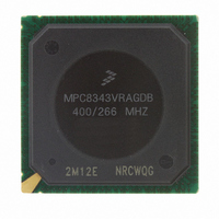
Manufacturer Part Number
MPC8343VRAGDB
Description
IC MPU POWERQUICC II 620-PBGA
Manufacturer
Freescale Semiconductor
Series
PowerQUICC II PROr
Datasheet
1.MPC8343VRAGDB.pdf
(79 pages)
Specifications of MPC8343VRAGDB
Processor Type
MPC83xx PowerQUICC II Pro 32-Bit
Speed
400MHz
Voltage
1.2V
Mounting Type
Surface Mount
Package / Case
620-PBGA
Processor Series
MPC8xxx
Core
e300
Data Bus Width
32 bit
Development Tools By Supplier
MPC8349E-MITXE
Maximum Clock Frequency
400 MHz
Maximum Operating Temperature
+ 105 C
Mounting Style
SMD/SMT
I/o Voltage
1.8 V, 2.5 V, 3.3 V
Minimum Operating Temperature
0 C
Core Size
32 Bit
Program Memory Size
64KB
Cpu Speed
400MHz
Embedded Interface Type
I2C, SPI, USB, UART
Digital Ic Case Style
BGA
No. Of Pins
620
Rohs Compliant
Yes
Family Name
MPC83xx
Device Core
PowerQUICC II Pro
Device Core Size
32b
Frequency (max)
400MHz
Instruction Set Architecture
RISC
Supply Voltage 1 (typ)
1.2V
Operating Supply Voltage (max)
1.26V
Operating Supply Voltage (min)
1.14V
Operating Temp Range
0C to 105C
Operating Temperature Classification
Commercial
Mounting
Surface Mount
Pin Count
620
Package Type
BGA
For Use With
CWH-PPC-8343N-VX - KIT EVAL SYSTEM QUICCSTART 8248CWH-PPC-8343N-VE - EVALUATION SYSTEM QUICC MPC8343E
Lead Free Status / RoHS Status
Lead free / RoHS Compliant
Features
-
Lead Free Status / Rohs Status
Lead free / RoHS Compliant
Available stocks
Company
Part Number
Manufacturer
Quantity
Price
Company:

Part Number:
MPC8343VRAGDB
Manufacturer:
Freescale Semiconductor
Quantity:
135
Company:
Part Number:
MPC8343VRAGDB
Manufacturer:
Freescale Semiconductor
Quantity:
10 000
Part Number:
MPC8343VRAGDB
Manufacturer:
FREESCALE
Quantity:
20 000


8.2.2
Table 27
Freescale Semiconductor
At recommended operating conditions with LV
Data to clock output skew (at transmitter)
Data to clock input skew (at receiver)
Clock cycle duration
Duty cycle for 1000Base-T
Duty cycle for 10BASE-T and 100BASE-TX
Rise time (20%–80%)
Fall time (80%–20%)
GTX_CLK125 reference clock period
GTX_CLK125 reference clock duty cycle
Notes:
1. In general, the clock reference symbol for this section is based on the symbols RGT to represent RGMII and RTBI timing. For
2. This implies that PC board design requires clocks to be routed so that an additional trace delay of greater than 1.5 ns is added
3. For 10 and 100 Mbps, t
4. Duty cycle may be stretched/shrunk during speed changes or while transitioning to a received packet clock domains as long
5. Duty cycle reference is LV
6. This symbol represents the external GTX_CLK125 and does not follow the original symbol naming convention.
example, the subscript of t
follows the clock symbol. For symbols representing skews, the subscript is SK followed by the clock being skewed (RGT).
to the associated clock signal.
as the minimum duty cycle is not violated and stretching occurs for no more than three t
presents the RGMII and RTBI AC timing specifications.
MPC8343EA PowerQUICC II Pro Integrated Host Processor Hardware Specifications, Rev. 10
RGMII and RTBI AC Timing
Parameter/Condition
3
RGT
4, 5
DD
RGT
scales to 400 ns ± 40 ns and 40 ns ± 4 ns, respectively.
/2.
Table 27. RGMII and RTBI AC Timing Specifications
represents the TBI (T) receive (RX) clock. Also, the notation for rise (R) and fall (F) times
2
DD
of 2.5 V ± 5%.
3, 5
Specifications
t
t
t
G125H
RGTH
RGTH
Symbol
t
t
t
SKRGT
SKRGT
t
t
t
RGTR
RGTF
G12
RGT
/t
/t
/t
RGT
RGT
6
G125
1
Ethernet: Three-Speed Ethernet, MII Management
–0.5
Min
1.0
7.2
45
40
47
—
—
—
RGT
of the lowest speed transitioned.
Typ
8.0
8.0
50
50
—
—
—
—
—
Max
0.75
0.75
0.5
2.8
8.8
55
60
53
—
Unit
ns
ns
ns
ns
ns
ns
%
%
%
25
Related parts for MPC8343VRAGDB
Image
Part Number
Description
Manufacturer
Datasheet
Request
R

Part Number:
Description:
Manufacturer:
Freescale Semiconductor, Inc
Datasheet:
Part Number:
Description:
Manufacturer:
Freescale Semiconductor, Inc
Datasheet:
Part Number:
Description:
Manufacturer:
Freescale Semiconductor, Inc
Datasheet:
Part Number:
Description:
Manufacturer:
Freescale Semiconductor, Inc
Datasheet:
Part Number:
Description:
Manufacturer:
Freescale Semiconductor, Inc
Datasheet:
Part Number:
Description:
Manufacturer:
Freescale Semiconductor, Inc
Datasheet:
Part Number:
Description:
Manufacturer:
Freescale Semiconductor, Inc
Datasheet:
Part Number:
Description:
Manufacturer:
Freescale Semiconductor, Inc
Datasheet:
Part Number:
Description:
Manufacturer:
Freescale Semiconductor, Inc
Datasheet:
Part Number:
Description:
Manufacturer:
Freescale Semiconductor, Inc
Datasheet:
Part Number:
Description:
Manufacturer:
Freescale Semiconductor, Inc
Datasheet:
Part Number:
Description:
Manufacturer:
Freescale Semiconductor, Inc
Datasheet:
Part Number:
Description:
Manufacturer:
Freescale Semiconductor, Inc
Datasheet:
Part Number:
Description:
Manufacturer:
Freescale Semiconductor, Inc
Datasheet:
Part Number:
Description:
Manufacturer:
Freescale Semiconductor, Inc
Datasheet: