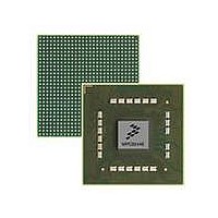
MPC8544VTALF Freescale Semiconductor, MPC8544VTALF Datasheet - Page 12

MPC8544VTALF
Manufacturer Part Number
MPC8544VTALF
Description
MPU POWERQUICC III 783-PBGA
Manufacturer
Freescale Semiconductor
Datasheets
1.MPC8544VTALF.pdf
(117 pages)
2.MPC8544VTALF.pdf
(2 pages)
3.MPC8544VTALF.pdf
(1340 pages)
Specifications of MPC8544VTALF
Processor Type
MPC85xx PowerQUICC III 32-Bit
Speed
667MHz
Voltage
1V
Mounting Type
Surface Mount
Package / Case
783-FCPBGA
Processor Series
MPC85xx
Core
e500
Data Bus Width
32 bit
Maximum Clock Frequency
667 MHz
Maximum Operating Temperature
+ 105 C
Mounting Style
SMD/SMT
Data Ram Size
32 KB
I/o Voltage
1.8 V, 3.3 V
Interface Type
I2C, HSSI, DUART
Minimum Operating Temperature
0 C
Lead Free Status / RoHS Status
Lead free / RoHS Compliant
Features
-
Lead Free Status / Rohs Status
Lead free / RoHS Compliant
Available stocks
Company
Part Number
Manufacturer
Quantity
Price
Company:
Part Number:
MPC8544VTALF
Manufacturer:
Freescale Semiconductor
Quantity:
10 000
Company:
Part Number:
MPC8544VTALFA
Manufacturer:
Freescale Semiconductor
Quantity:
10 000
Electrical Characteristics
2.1.3
Table 3
2.2
The device requires its power rails to be applied in specific sequence in order to ensure proper device
operation. These requirements are as follows for power up:
Note that all supplies must be at their stable values within 50 ms.
Items on the same line have no ordering requirement with respect to one another. Items on separate lines
must be ordered sequentially such that voltage rails on a previous step must reach 90% of their value before
the voltage rails on the current step reach 10% of theirs.
In order to guarantee MCKE low during power-up, the above sequencing for GV
no concern about any of the DDR signals being in an indeterminate state during power up, then the
sequencing for GV
From a system standpoint, if any of the I/O power supplies ramp prior to the V
associated with that I/O supply may drive a logic one or zero during power-up, and extra current may be
drawn by the device.
12
Local bus interface utilities signals
PCI signals
DDR signal
DDR2 signal
TSEC signals
DUART, system control, JTAG
I
Notes:
1. The drive strength of the local bus interface is determined by the configuration of the appropriate bits in PORIMPSCR.
2. The drive strength of the PCI interface is determined by the setting of the PCI_GNT1 signal at reset.
2
C
1. V
2. GV
provides information on the characteristics of the output driver strengths.
DD
Power Sequencing
DD
Output Driver Characteristics
, AV
MPC8544E PowerQUICC III Integrated Processor Hardware Specifications, Rev. 5
DD
DD
_n, BV
Driver Type
is not required.
DD
, LV
DD
Table 3. Output Drive Capability
, SV
DD
, OV
DD
, TV
32 (half strength mode)
Output Impedance
DD
Programmable
, XV
45 (default)
45 (default)
42 (default)
125
150
(Ω)
25
35
25
20
16
42
42
DD
DD
LV
OV
GV
GV
OV
OV
DD
BV
BV
BV
BV
BV
DD
core supply, the I/Os
Voltage
Supply
DD
DD
DD
DD
DD
is required. If there is
DD
DD
DD
DD
DD
Freescale Semiconductor
= 2.5/3.3 V
= 3.3 V
= 2.5 V
= 3.3 V
= 2.5 V
= 1.8 V
= 3.3 V
= 3.3 V
= 3.3 V
= 2.5 V
= 1.8 V
Notes
—
—
—
—
—
1
2


