MC68EC020FG25 Freescale Semiconductor, MC68EC020FG25 Datasheet - Page 266
MC68EC020FG25
Manufacturer Part Number
MC68EC020FG25
Description
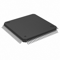
IC MPU 32 BIT 25MHZ 100-QFP
Manufacturer
Freescale Semiconductor
Datasheet
1.MC68EC020AA16.pdf
(306 pages)
Specifications of MC68EC020FG25
Processor Type
M680x0 32-Bit
Speed
25MHz
Voltage
5V
Mounting Type
Surface Mount
Package / Case
100-QFP
Lead Free Status / RoHS Status
Contains lead / RoHS non-compliant
Features
-
Available stocks
Company
Part Number
Manufacturer
Quantity
Price
Company:

Part Number:
MC68EC020FG25
Manufacturer:
FREESCALE
Quantity:
8 831
Company:
Part Number:
MC68EC020FG25
Manufacturer:
Freescale Semiconductor
Quantity:
10 000
Part Number:
MC68EC020FG25
Manufacturer:
MOTOROL
Quantity:
20 000


9.6 ACCESS TIME CALCULATIONS
The timing paths that are critical in any memory interface are illustrated and defined in
Figure 9-9.
The type of device that is interfaced to the MC68020/EC020 determines exactly which of
the paths is most critical. The address-to-data paths are typically the critical paths for
static devices since there is no penalty for initiating a cycle to these devices and later
validating that access with the appropriate bus control signal. Conversely, the address-
strobe-to-data-valid path is often most critical for dynamic devices since the cycle must be
validated before an access can be initiated. For devices that signal termination of a bus
cycle before data is validated (e.g., error detection and correction hardware and some
external caches), to improve performance, the critical path may be from the address or
strobes to the assertion of BERR (or BERR and HALT ). Finally, the address-valid-to-
DSACK1/DSACK0- asserted path is most critical for very fast devices and external
caches, since the time available between the address becoming valid and the
DSACK1/DSACK0 assertion to terminate the bus cycle is minimal. Table 9-4 provides
the equations required to calculate the various memory access times assuming a 50-
percent duty cycle clock.
9-12
*
NOTE: This diagram illustrates access time calculations only
DSACK1/DSACK0
For the MC68EC020, A23–A0.
BERR, HALT
Parameter
*
D31–D0
A31–A0
a
b
c
d
e
CLK
f
AS
Address Valid to DSACK1/DSACK0 Asserted
AS Asserted to DSACK1/DSACK0 Asserted
Address Valid to BERR/HALT Asserted
AS Asserted to BERR/HALT Asserted
Address Valid to Data Valid
AS Asserted to Data Valid
S0
S1
Description
M68020 USER’S MANUAL
S2
a
b
d
c
System
t AVBHL
t SABHL
t AVDL
t SADL
t AVDV
t SADV
e
f
Equation
9-3
9-4
9-5
9-6
9-7
9-8
S0
MOTOROLA
Related parts for MC68EC020FG25
Image
Part Number
Description
Manufacturer
Datasheet
Request
R

Part Number:
Description:
Manufacturer:
Freescale Semiconductor, Inc
Datasheet:
Part Number:
Description:
Manufacturer:
Freescale Semiconductor, Inc
Datasheet:
Part Number:
Description:
Manufacturer:
Freescale Semiconductor, Inc
Datasheet:
Part Number:
Description:
Manufacturer:
Freescale Semiconductor, Inc
Datasheet:
Part Number:
Description:
Manufacturer:
Freescale Semiconductor, Inc
Datasheet:
Part Number:
Description:
Manufacturer:
Freescale Semiconductor, Inc
Datasheet:
Part Number:
Description:
Manufacturer:
Freescale Semiconductor, Inc
Datasheet:
Part Number:
Description:
Manufacturer:
Freescale Semiconductor, Inc
Datasheet:
Part Number:
Description:
Manufacturer:
Freescale Semiconductor, Inc
Datasheet:
Part Number:
Description:
Manufacturer:
Freescale Semiconductor, Inc
Datasheet:
Part Number:
Description:
Manufacturer:
Freescale Semiconductor, Inc
Datasheet:
Part Number:
Description:
Manufacturer:
Freescale Semiconductor, Inc
Datasheet:
Part Number:
Description:
Manufacturer:
Freescale Semiconductor, Inc
Datasheet:
Part Number:
Description:
Manufacturer:
Freescale Semiconductor, Inc
Datasheet:
Part Number:
Description:
Manufacturer:
Freescale Semiconductor, Inc
Datasheet: