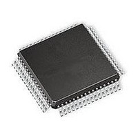
ST92T163R4T1 STMicroelectronics, ST92T163R4T1 Datasheet - Page 197

ST92T163R4T1
Manufacturer Part Number
ST92T163R4T1
Description
Microcontrollers (MCU) OTP EPROM 20K USB/I2
Manufacturer
STMicroelectronics
Datasheet
1.ST92T163R4T1.pdf
(224 pages)
Specifications of ST92T163R4T1
Data Bus Width
8 bit, 16 bit
Program Memory Type
EPROM
Program Memory Size
20 KB
Data Ram Size
2 KB
Interface Type
I2C, SCI, USB
Maximum Clock Frequency
24 MHz
Number Of Programmable I/os
64
Number Of Timers
2
Operating Supply Voltage
4 V to 5.5 V
Maximum Operating Temperature
+ 70 C
Mounting Style
SMD/SMT
Package / Case
TQFP-64
Minimum Operating Temperature
0 C
On-chip Adc
8 bit
Lead Free Status / Rohs Status
No
Available stocks
Company
Part Number
Manufacturer
Quantity
Price
Company:
Part Number:
ST92T163R4T1L
Manufacturer:
ST
Quantity:
444
Part Number:
ST92T163R4T1L
Manufacturer:
ST
Quantity:
20 000
8.6 A/D CONVERTER (A/D)
8.6.1 Introduction
The 8 bit Analog to Digital Converter uses a fully
differential analog configuration for the best noise
immunity and precision performance. The analog
voltage references of the converter are connected
to the internal AV
the chip if they are available, otherwise to the ordi-
nary V
guaranteed accuracy depends on the device (see
Electrical Characteristics). A fast Sample/Hold al-
lows quick signal sampling for minimum warping
effect and conversion error.
8.6.2 Main Features
Figure 86. A/D Converter Block Diagram
n
8-bit resolution A/D Converter
Single Conversion Time (including Sampling
Time):
– 138 internal system clock periods in slow
– 78 INTCLK periods in fast mode (~6.5 s @
Sample/Hold: Tsample=
– 84 INTCLK periods in slow mode (~3.4
– 48 INTCLK periods in fast mode (~4
Up to 8 Analog Inputs (the number of inputs is
device dependent, see device pinout)
mode (~5.6
clock);
12MHZ internal system clock)
@25Mhz internal system clock)
@12Mhz internal system clock)
DD
and V
SS
DD
s @25Mhz internal system
supply pins of the chip. The
& AV
REGIST ER
DATA
SS
analog supply pins of
APPROXI MATION
SUCCE SSIVE
REGISTER
CONTROL LOGIC
s
s
S/H
8.6.3 General Description
Depending on the device, up to 8 analog inputs
can be selected by software.
Different conversion modes are provided: single,
continuous, or triggered. The continuous mode
performs a continuous conversion flow of the se-
lected channel, while in the single mode the se-
lected channel is converted once and then the log-
ic waits for a new hardware or software restart.
A data register (ADDTR) is available, mapped in
page 62, allowing data storage (in single or contin-
uous mode).
The start conversion event can be managed by
software, writing the START/STOP bit of the Con-
trol Logic Register or by hardware using either:
– An external signal on the EXTRG triggered input
– An On Chip Event generated by another periph-
(negative edge sensitive) connected as an Alter-
nate Function to an I/O port bit
eral, such as the MFT (Multifunction Timer).
Single/Continuous Conversion Mode
External/Internal source
synchronization)
Power Down mode (Zero Power Consumption)
1 Control Logic Register
1 Data Register
ST92163 - A/D CONVERTER (A/D)
ANALOG
(On Chip Event)
MUX
INTRG
Trigger
EXTRG
Ain0
Ain1
Ainx
(Alternate
197/224


