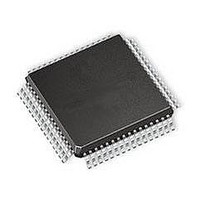
ST92T163R4T1 STMicroelectronics, ST92T163R4T1 Datasheet - Page 199

ST92T163R4T1
Manufacturer Part Number
ST92T163R4T1
Description
Microcontrollers (MCU) OTP EPROM 20K USB/I2
Manufacturer
STMicroelectronics
Datasheet
1.ST92T163R4T1.pdf
(224 pages)
Specifications of ST92T163R4T1
Data Bus Width
8 bit, 16 bit
Program Memory Type
EPROM
Program Memory Size
20 KB
Data Ram Size
2 KB
Interface Type
I2C, SCI, USB
Maximum Clock Frequency
24 MHz
Number Of Programmable I/os
64
Number Of Timers
2
Operating Supply Voltage
4 V to 5.5 V
Maximum Operating Temperature
+ 70 C
Mounting Style
SMD/SMT
Package / Case
TQFP-64
Minimum Operating Temperature
0 C
On-chip Adc
8 bit
Lead Free Status / Rohs Status
No
Available stocks
Company
Part Number
Manufacturer
Quantity
Price
Company:
Part Number:
ST92T163R4T1L
Manufacturer:
ST
Quantity:
444
Part Number:
ST92T163R4T1L
Manufacturer:
ST
Quantity:
20 000
A/D CONVERTER (Cont’d)
8.6.4 Register Description
A/D CONTROL LOGIC REGISTER (ADCLR)
R241 - Read/Write
Register Page: 62
Reset value: 0000 0000 (00h)
This 8-bit register manages the A/D logic opera-
tions. Any write operation to it will cause the cur-
rent conversion to be aborted and the logic to be
re-initialized to the starting configuration.
Bit 7:5 = C[2:0]: Channel Address.
These bits are set and cleared by software. They
select channel i conversion as follows:
Bit 4 = FS: Fast/Slow .
This bit is set and cleared by software.
0: Fast mode. Single conversion time: 78 x
1: Slow mode. Single conversion time: 138 x
Note: Fast conversion mode is only allowed for in-
ternal speeds which do not exceed 12 MHz.
Bit 3 = TRG: External/Internal Trigger Enable .
This bit is set and cleared by software.
0: External/Internal Trigger disabled.
1: Either a negative (falling) edge on the EXTRG
C2
C2
INTCLK (5.75 s at INTCLK = 12 MHz)
INTCLK (11.5 s at INTCLK = 12 MHz)
pin or an On Chip Event writes a “1” into the
STR bit, enabling start of conversion.
7
0
0
0
0
1
1
1
1
C1
C1
0
0
1
1
0
0
1
1
C0
C0
0
1
0
1
0
1
0
1
FS
TRG POW CONT STR
Channel Enabled
Channel 0
Channel 1
Channel 2
Channel 3
Channel 4
Channel 5
Channel 6
Channel 7
0
Note: Triggering by on chip event is available on
devices with the multifunction timer (MFT) periph-
eral.
Bit 2 = POW: Power Enable .
This bit is set and cleared by software.
0: Disables all power consuming logic.
1: Enables the A/D logic and analog circuitry.
Bit 1 = CONT: Continuous/Single Mode Select .
This bit it set and cleared by software.
0: Single mode: after the current conversion ends,
1: Select Continuous Mode, a continuous flow of
Bit 0 = STR: Start/Stop .
This bit is set and cleared by software. It is also set
by hardware when the A/D is synchronized with an
external/internal trigger.
0: Stop conversion on channel i. An interrupt is
1: Start conversion on channel i
WARNING: When accessing this register, it is rec-
ommended to keep the related A/D interrupt chan-
nel masked or disabled to avoid spurious interrupt
requests.
A/D CHANNEL i DATA REGISTER (ADDTR)
R240 - Read/Write
Register Page: 62
Reset value: undefined
The result of the conversion of the selected chan-
nel is stored in the 8-bit ADDTR, which is reloaded
with a new value every time a conversion ends.
R.7
the STR bit is reset by hardware and the con-
verter logic is put in a wait status. To start anoth-
er conversion, the STR bit has to be set by soft-
ware or hardware.
A/D conversions on the selected channel, start-
ing when the STR bit is set.
generated if the STR was previously set and the
AD-INT bit is set.
7
R.6
ST92163 - A/D CONVERTER (A/D)
R.5
R.4
R.3
R.2
R.1
199/224
R.0
0


