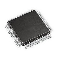
ST92T163R4T1 STMicroelectronics, ST92T163R4T1 Datasheet - Page 98

ST92T163R4T1
Manufacturer Part Number
ST92T163R4T1
Description
Microcontrollers (MCU) OTP EPROM 20K USB/I2
Manufacturer
STMicroelectronics
Datasheet
1.ST92T163R4T1.pdf
(224 pages)
Specifications of ST92T163R4T1
Data Bus Width
8 bit, 16 bit
Program Memory Type
EPROM
Program Memory Size
20 KB
Data Ram Size
2 KB
Interface Type
I2C, SCI, USB
Maximum Clock Frequency
24 MHz
Number Of Programmable I/os
64
Number Of Timers
2
Operating Supply Voltage
4 V to 5.5 V
Maximum Operating Temperature
+ 70 C
Mounting Style
SMD/SMT
Package / Case
TQFP-64
Minimum Operating Temperature
0 C
On-chip Adc
8 bit
Lead Free Status / Rohs Status
No
Available stocks
Company
Part Number
Manufacturer
Quantity
Price
Company:
Part Number:
ST92T163R4T1L
Manufacturer:
ST
Quantity:
444
Part Number:
ST92T163R4T1L
Manufacturer:
ST
Quantity:
20 000
ST92163 - I/O PORTS
7 I/O PORTS
7.1 INTRODUCTION
ST9 devices feature flexible individually program-
mable multifunctional input/output lines. Refer to
the Pin Description Chapter for specific pin alloca-
tions. These lines, which are logically grouped as
8-bit ports, can be individually programmed to pro-
vide digital input/output and analog input, or to
connect input/output signals to the on-chip periph-
erals as alternate pin functions. All ports can be in-
dividually configured as an input, bi-directional,
output or alternate function. In addition, pull-ups
can be turned off for open-drain operation, and
weak pull-ups can be turned on in their place, to
avoid the need for off-chip resistive pull-ups. Ports
configured as open drain must never have voltage
on the port pin exceeding V
cal Characteristics section). Input buffers can be
either TTL or CMOS compatible. Alternatively
some input buffers can be permanently forced by
hardware to operate as Schmitt triggers.
Figure 54. I/O Register Map
98/224
E5h
E4h
E3h
E2h
E1h
E0h
GROUP E
Registers
System
P5DR
P4DR
P3DR
P2DR
P1DR
P0DR
DD
R229
R228
R227
R226
R225
R224
(refer to the Electri-
FFh
FEh
FDh
FCh
FBh
FAh
F9h
F8h
F7h
F6h
F5h
F4h
F3h
F2h
F1h
F0h
GROUP F
Reserved
Reserved
Reserved
Reserved
PAGE 2
P3C2
P3C1
P3C0
P2C2
P2C1
P2C0
P1C2
P1C1
P1C0
P0C2
P0C1
P0C0
7.2 SPECIFIC PORT CONFIGURATIONS
Refer to the Pin Description chapter for a list of the
specific port styles and reset values.
7.3 PORT CONTROL REGISTERS
Each port is associated with a Data register
(PxDR) and three Control registers (PxC0, PxC1,
PxC2). These define the port configuration and al-
low dynamic configuration changes during pro-
gram execution. Port Data and Control registers
are mapped into the Register File as shown in Fig-
ure 54. Port Data and Control registers are treated
just like any other general purpose register. There
are no special instructions for port manipulation:
any instruction that can address a register, can ad-
dress the ports. Data can be directly accessed in
the port register, without passing through other
memory or “accumulator” locations.
GROUP F
Reserved
Reserved
PAGE 3
P7DR
P6DR
P7C2
P7C1
P7C0
P6C2
P6C1
P6C0
P5C2
P5C1
P5C0
P4C2
P4C1
P4C0
GROUP F
PAGE 43
Reserved
P9DR
P8DR
P9C2
P9C1
P9C0
P8C2
P8C1
P8C0
R255
R254
R253
R252
R251
R250
R249
R248
R247
R246
R245
R244
R243
R242
R241
R240


