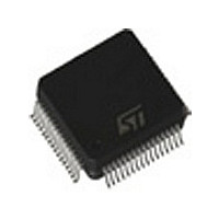
STV0299B STMicroelectronics, STV0299B Datasheet - Page 7

STV0299B
Manufacturer Part Number
STV0299B
Description
Manufacturer
STMicroelectronics
Datasheet
1.STV0299B.pdf
(36 pages)
Specifications of STV0299B
Pin Count
64
Screening Level
Commercial
Lead Free Status / Rohs Status
Specific Sites Compliant
Available stocks
Company
Part Number
Manufacturer
Quantity
Price
Part Number:
STV0299B
Manufacturer:
ST
Quantity:
20 000
Company:
Part Number:
STV0299BL
Manufacturer:
MICRON
Quantity:
10 000
Part Number:
STV0299BLT
Manufacturer:
ST
Quantity:
20 000
4
The STV0299B is a multistandard demodulator
and error correction decoder IC for the reception
of QPSK and BPSK modulated signals. It is
intended for use in digital satellite television
applications. The IC can accept two standards of
QPSK modulated signals (DVB and DSS) as well
as BPSK modulated signals over a wide symbol
frequency range (from 1 to 50 Msymbols/s). The
signals are digitized via an integrated dual 6-bit
analog to digital converter, and interpolated and
digitally filtered by a Nyquist root filter (with a
settable roll-off value of either 0.35 or 0.20).
There are two built-in digital Automatic Gain
Controls (AGCs). The first AGC allows the tuner
gain to be controlled by the pulse density
modulated output. The second AGC performs
power optimization of the digital signal bandwidth
(internal to the STV0299B). The digital signal then
passes through the digital carrier loop fitted with
an on-chip derotator and tracking loop, lock
detector, and digital timing recovery.
Forward error correction is integrated by way of an
inner
Reed-Solomon decoder.
4.1 Front End Interfaces
4.1.1
The standard I
first byte is Hex D0 for a write operation, or Hex
D1 for a read operation. The I
operates differently depending on whether it is in
normal or standby mode.
Figure 2:
Figure 3:
Write registers 0 to 3 with AA, BB, CC, DD
Read registers 2 and 3
Write operation
Read operation
Note: 1 ACK is not absolutely necessary after Data
Start
Start
Start
Start
Start
Start
FUNCTIONAL DESCRIPTION
Viterbi
I
2
C Interface
Address,
Write D0
Device Address, Write D0
Device Address, Write D0
Device
I
I
2
2
C Read and Write Operations in Normal Mode
C Read and Write Operations in Standby Mode
Device Address,
Device Address,
Device Address
2
soft
C protocol is used whereby the
, Read D0
Read D1
Read D1
ACK
decoder,
Register
Address
00
and
ACK
ACK
ACK
ACK
ACK
2
ACK
C interface
an
Register Address 02
Register Address 01, 02 or 03
Data
Data Read CC
outer
AA
Register Address
Reader Data
ACK
4.1.2
The byte sequence is as follows:
1 The first byte gives the device address plus the
2 The second byte contains the internal address
3 The next byte is written in the internal register.
4 The transfer lasts until stop conditions are
5 The STV0299B acknowledges every byte
4.1.3
The address of the first register to read is
programmed in a write operation without data, and
terminated by the stop condition. Then, another
start is followed by the device address and R/
W = 1. All following bytes are now data to be read
at successive positions starting from the initial
address. Figure 2 shows the I
Write and Read Registers.
4.1.4
Only three registers can be addressed while in
standby mode: RCR (address 01 Hex), MCR
(address 02 Hex) and ACR (address 03 Hex).
These three registers can be either read or written
to (refer to Figure 3).
Only one register may be read or written to per
sequence (no increment). While in standby mode,
the Serial Clock (SCL) frequency must be lower than
one tenth of the CLK_IN frequency (f
direction bit (R/W = 0).
of the first register to be accessed.
Following
successive internal registers.
encountered.
transfer.
Data
BB
ACK
ACK
Write Operation (Normal Mode)
Read Operation (Normal Mode)
I
2
C Interface in Standby Mode
ACK
Stop
bytes
ACK (or no
ACK
ACK
Data
ACK
CC
Data Read DD
1
)
(if
ACK
Data
any)
Stop
Stop
Data
DD
2
C Normal Mode
are
ACK
CLK_IN
STV0299B
ACK
ACK
written
Stop
/ 10).
Stop
Stop
7/36
in


