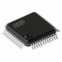
SC16C652BIB48,151 NXP Semiconductors, SC16C652BIB48,151 Datasheet - Page 7

SC16C652BIB48,151
Manufacturer Part Number
SC16C652BIB48,151
Description
IC UART DUAL W/FIFO 48-LQFP
Manufacturer
NXP Semiconductors
Type
IrDAr
Datasheet
1.SC16C652BIB48151.pdf
(43 pages)
Specifications of SC16C652BIB48,151
Number Of Channels
2, DUART
Package / Case
48-LQFP
Features
2 Channels
Fifo's
32 Byte
Voltage - Supply
2.5V, 3.3V, 5V
With Auto Flow Control
Yes
With Irda Encoder/decoder
Yes
With False Start Bit Detection
Yes
With Modem Control
Yes
With Cmos
Yes
Mounting Type
Surface Mount
Data Rate
5 Mbps
Supply Voltage (max)
5.5 V
Supply Voltage (min)
2.25 V
Supply Current
4.5 mA
Maximum Operating Temperature
+ 85 C
Minimum Operating Temperature
- 40 C
Mounting Style
SMD/SMT
Operating Supply Voltage
2.5 V or 3.3 V or 5 V
Lead Free Status / RoHS Status
Lead free / RoHS Compliant
Lead Free Status / RoHS Status
Lead free / RoHS Compliant, Lead free / RoHS Compliant
Other names
568-3276
935274409151
SC16C652BIB48-S
935274409151
SC16C652BIB48-S
Available stocks
Company
Part Number
Manufacturer
Quantity
Price
Company:
Part Number:
SC16C652BIB48,151
Manufacturer:
NXP Semiconductors
Quantity:
10 000
Philips Semiconductors
Table 2:
6. Functional description
SC16C652B_4
Product data sheet
Symbol
V
XTAL1
XTAL2
CC
42
13
14
LQFP48 HVQFN32
Pin description
Pin
26
10
11
The SC16C652B provides serial asynchronous receive data synchronization,
parallel-to-serial and serial-to-parallel data conversions for both the transmitter and
receiver sections. These functions are necessary for converting the serial data stream into
parallel data that is required with digital data systems. Synchronization for the serial data
stream is accomplished by adding start and stop bits to the transmit data to form a data
character (character orientated protocol). Data integrity is insured by attaching a parity bit
to the data character. The parity bit is checked by the receiver for any transmission bit
errors. The electronic circuitry to provide all these functions is fairly complex, especially
when manufactured on a single integrated silicon chip. The SC16C652B represents such
an integration with greatly enhanced features. The SC16C652B is fabricated with an
advanced CMOS process.
The SC16C652B is an upward solution that provides a dual UART capability with 32 bytes
of transmit and receive FIFO memory, instead of 16 bytes for the 16C2550 and none in
the 16C2450. The SC16C652B is designed to work with high speed modems and shared
network environments that require fast data processing time. Increased performance is
realized in the SC16C652B by the transmit and receive FIFOs. This allows the external
processor to handle more networking tasks within a given time. In addition, the four
selectable receive and transmit FIFO trigger interrupt levels are uniquely provided for
maximum data throughput performance especially when operating in a multi-channel
environment. The FIFO memory greatly reduces the bandwidth requirement of the
external controlling CPU, increases performance, and reduces power consumption.
The SC16C652B is capable of operation up to 5 Mbit/s with a 80 MHz clock. With a crystal
or external clock input of 7.3728 MHz, the user can select data rates up to 460.8 kbit/s.
The rich feature set of the SC16C652B is available through internal registers. Selectable
receive and transmit FIFO trigger levels, selectable TX and RX baud rates, and modem
interface controls are all standard features. Following a power-on reset or an external
reset, the SC16C652B is software compatible with the previous generation, SC16C2550
and ST16C2450.
…continued
Type Description
I
I
O
Power supply input.
Crystal or external clock input. Functions as a crystal input or as an external
clock input. A crystal can be connected between this pin and XTAL2 to form an
internal oscillator circuit. This configuration requires an external 1 M resistor
between the XTAL1 and XTAL2 pins. Alternatively, an external clock can be
connected to this pin to provide custom data rates (see
“Programmable baud rate
Output of the crystal oscillator or buffered clock. (See also XTAL1.) Crystal
oscillator output or buffered clock output. Should be left open if an external clock is
connected to XTAL1. For extended frequency operation, this pin should be tied to
V
CC
via a 2 k resistor.
Rev. 04 — 1 September 2005
Dual UART with 32-byte FIFOs and IrDA encoder/decoder
generator”). See
Figure
© Koninklijke Philips Electronics N.V. 2005. All rights reserved.
4.
SC16C652B
Section 6.8
7 of 43


