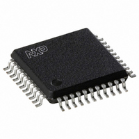
SC28L92A1B,557 NXP Semiconductors, SC28L92A1B,557 Datasheet - Page 53

SC28L92A1B,557
Manufacturer Part Number
SC28L92A1B,557
Description
IC UART DUAL W/FIFO 44-PQFP
Manufacturer
NXP Semiconductors
Series
IMPACTr
Type
Dual UARTr
Datasheet
1.SC28L92A1B557.pdf
(73 pages)
Specifications of SC28L92A1B,557
Number Of Channels
2, DUART
Package / Case
44-MQFP, 44-PQFP
Features
False-start Bit Detection
Fifo's
16 Byte
Voltage - Supply
3.3V, 5V
With Auto Flow Control
Yes
With False Start Bit Detection
Yes
With Modem Control
Yes
With Cmos
Yes
Mounting Type
Surface Mount
Data Rate
0.2304 MBd
Supply Voltage (max)
3.63 V or 5.5 V
Supply Voltage (min)
2.97 V or 4.5 V
Supply Current
25 mA
Maximum Operating Temperature
+ 85 C
Minimum Operating Temperature
- 40 C
Mounting Style
SMD/SMT
Operating Supply Voltage
3.3 V or 5 V
Lead Free Status / RoHS Status
Lead free / RoHS Compliant
Lead Free Status / RoHS Status
Lead free / RoHS Compliant, Lead free / RoHS Compliant
Other names
568-1211
935263294557
SC28L92A1B
935263294557
SC28L92A1B
Available stocks
Company
Part Number
Manufacturer
Quantity
Price
Company:
Part Number:
SC28L92A1B,557
Manufacturer:
NXP Semiconductors
Quantity:
10 000
NXP Semiconductors
Table 66.
V
[1]
[2]
[3]
[4]
SC28L92_7
Product data sheet
Symbol
V
V
V
V
I
I
I
I
I
I
I
I
I
I(1XPD)
IL(X1)
IH(X1)
I
OZH
OZL
ODL
ODH
CC
CC
IL
IH
OL
OH
= 3.3 V
The following conditions apply:
a) Parameters are valid over specified temperature and voltage range.
b) All voltage measurements are referenced to ground. For testing, all inputs swing between 0.4 V and 3.0 V with a transition time of
c) Typical values are at 25 C, typical supply voltages, and typical processing parameters.
Test conditions for outputs: C
constant current source = 2.6 mA.
Input port pins have active pull-up transistors that will source a typical 2 A from V
0.0 A.
All outputs are disconnected. Inputs are switching between CMOS levels of V
5 ns maximum. For X1/CLK this swing is between 0.4 V and 0.8V
and 2.0 V, and output voltages of 0.8 V and 2.0 V, as appropriate.
Static characteristics, 3.3 V operation
10 %; T
Parameter
input LOW voltage
input HIGH voltage
output LOW voltage
output HIGH voltage
Power-down mode input
current on pin X1/CLK
operating input LOW current
on pin X1/CLK
operating input HIGH current
on pin X1/CLK
input leakage current
output off current HIGH,
3-state data bus
output off current LOW, 3-state
data bus
open-drain output LOW current
in off state
open-drain output HIGH
current in off state
power supply current
amb
= 40 C to +85 C; unless otherwise specified.
L
= 125 pF, except interrupt outputs. Test conditions for interrupt outputs: C
Conditions
I
except open-drain outputs;
I
V
V
V
V
V
V
V
V
CMOS input levels
Rev. 07 — 19 December 2007
OL
OH
I
I
I
I
I
I
I
I
3.3 V/5.0 V Dual Universal Asynchronous Receiver/Transmitter
all except input port pins
input port pins
operating mode
Power-down mode
= 0 V to V
= 0 V
= V
= 0 V to V
= V
= 0 V
= 0 V
= V
= 2.4 mA
= 400 A
[1]
CC
CC
CC
CC
CC
CC
. All time measurements are referenced at input voltages of 0.8 V
CC
CC
0.2 V and V
when they are at V
[2]
[3]
[3]
[4]
Min
-
0.8V
-
V
0
-
-
-
-
0.5
80
0.5
8
0.5
0.5
CC
SS
CC
+ 0.2 V.
0.5 V
SS
L
Typ
0.65
1.7
0.2
+0.05
-
-
+0.05
+0.5
-
-
-
-
-
. Input port pins at V
= 125 pF,
1
CC
SC28L92
0.2 -
© NXP B.V. 2007. All rights reserved.
Max
0.2V
-
0.4
+0.5
0
80
+0.5
+0.5
0.5
-
-
0.5
5
5.0
CC
CC
53 of 73
Unit
V
V
V
V
mA
source
A
A
A
A
A
A
A
A
A
A


