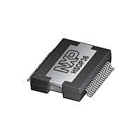
TDF8599A NXP Semiconductors, TDF8599A Datasheet - Page 11

TDF8599A
Manufacturer Part Number
TDF8599A
Description
The TDF8599A is a dual Bridge-Tied Load (BTL) car audio amplifier comprising anNDMOST-NDMOST output stage based on SOI BCDMOS technology
Manufacturer
NXP Semiconductors
Datasheet
1.TDF8599A.pdf
(54 pages)
Available stocks
Company
Part Number
Manufacturer
Quantity
Price
Part Number:
TDF8599ATD
Manufacturer:
NXP/恩智浦
Quantity:
20 000
Part Number:
TDF8599ATH
Manufacturer:
NXP/恩智浦
Quantity:
20 000
NXP Semiconductors
TDF8599A_2
Product data sheet
8.4.1 Modulation mode
8.4 Operation mode selection
Pin MOD is used to select specific operating modes. The resistor (R
between pins MOD and AGND together with the non-I
operating mode (see
mode or I
between pins ADS and AGND.
In non-I
In I
mode and phase shift are programmed using I
Table 8.
[1]
[2]
[3]
In I
amplifier switching interference generating incorrect information on pin MOD.
In non-I
one of the TDF8599A’s outputs starts switching.
In non-I
Table
Figure 10
R
0 (short to AGND) Stereo mode
4.7
13
33
100
•
•
•
•
•
MOD
(open)
2
2
AD or BD modulation (see
1
Parallel mode operation (see
C-bus mode, pin MOD can only select Parallel mode. In addition, the modulation
R
R
See
C-bus mode, pin MOD is latched using the I
AD modulation mode: the bridge halves switch in opposite phase.
BD modulation mode: the bridge halves switch in phase but the input signal for the
modulators is inverted.
2
ADS
ADS
8). In I
(k )
2
2
2
Section 8.4.3 on page 14
C-bus mode, pin MOD is used to select:
C-bus mode or when IB3[D7] = 0, the information on pin MOD is latched when
C-bus mode, pin MOD is used to select either AD or BD modulation mode (see
= 0 ; pin ADS is short circuited to pin AGND.
phase shift when oscillator is used in Slave mode (see
2
4.7 k ; See
and
C-bus mode is active. This in turn is determined by the resistor value connected
Operation mode selection with the MOD pin
2
C-bus mode, the modulation mode is selected using an I
Figure 11
I
Parallel mode
2
C-bus mode
Table 13 on page
Table
Rev. 02 — 30 June 2009
show simplified representations of AD and BD modulation.
8). The mode of operation depends on whether non-I
for more detailed information.
I
2
[3]
Section
C-bus controlled dual channel class-D power amplifier
[1]
Section
23.
8.4.1).
8.4.3).
Non-I
AD modulation: no phase shift in Slave mode
BD modulation: no phase shift in Slave mode
AD modulation:
BD modulation:
AD modulation: no phase shift in Slave mode
BD modulation: no phase shift in Slave mode
2
2
C-bus commands.
2
C-bus command IB3[D7] = 1. This avoids
C-bus mode
2
C-bus/I
1
1
2
2
[2]
phase shift in Slave mode
phase shift in Slave mode
2
C-bus mode determine the
Section
TDF8599A
MOD
2
C-bus command.
© NXP B.V. 2009. All rights reserved.
) connected
8.4.2).
2
C-bus
11 of 54


