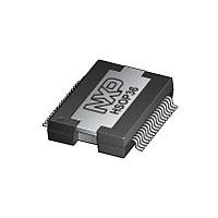
TDF8599A NXP Semiconductors, TDF8599A Datasheet - Page 5

TDF8599A
Manufacturer Part Number
TDF8599A
Description
The TDF8599A is a dual Bridge-Tied Load (BTL) car audio amplifier comprising anNDMOST-NDMOST output stage based on SOI BCDMOS technology
Manufacturer
NXP Semiconductors
Datasheet
1.TDF8599A.pdf
(54 pages)
Available stocks
Company
Part Number
Manufacturer
Quantity
Price
Part Number:
TDF8599ATD
Manufacturer:
NXP/恩智浦
Quantity:
20 000
Part Number:
TDF8599ATH
Manufacturer:
NXP/恩智浦
Quantity:
20 000
NXP Semiconductors
8. Functional description
TDF8599A_2
Product data sheet
8.1 General
Table 3.
[1]
[2]
The TDF8599A is a dual full bridge (BTL) audio power amplifier using class-D technology.
The audio input signal is converted into a Pulse-Width Modulated (PWM) signal using the
analog input and PWM control stages. A PWM signal is applied to driver circuits for both
high-side and low-side enabling the DMOS power output transistors to be driven. An
external 2
across the loudspeakers.
Symbol
CLIP
DIAG
SDA
SCL
SSM
OSCSET
OSCIO
DCP
VSTAB2
OUT2N
BOOT2N
V
PGND2
BOOT2P
OUT2P
OUT1P
BOOT1P
PGND1
V
BOOT1N
OUT1N
VSTAB1
V
GNDD/HW
P2
P1
DDD
[2]
[2]
I = input, O = output, I/O = input/output, G = ground and P = power supply.
In this data sheet supply voltage V
nd
Pin description
order low-pass filter converts the PWM signal into an analog audio signal
Pin
13
14
15
16
17
18
19
20
21
22
23
24
25
26
27
28
29
30
31
32
33
34
35
36
Type
O
O
I/O
I
I/O
I
O
P
G
O
O
G
P
O
G
Rev. 02 — 30 June 2009
…continued
[1]
I
2
C-bus controlled dual channel class-D power amplifier
P
Description
clip output; open-drain
diagnostic output; open-drain
I
I
master setting: Spread spectrum mode frequency
slave setting: phase lock operation
master/slave oscillator setting
master only setting: set internal oscillator frequency
external oscillator slave setting: input
internal oscillator master setting: output
DC protection input for the filtered output voltages
decoupling internal stabilizer 2 for DMOST drivers
channel 2 negative PWM output
boot 2 negative bootstrap capacitor
channel 2 power supply voltage
channel 2 power ground
boot 2 positive bootstrap capacitor
channel 2 positive PWM output
channel 1 positive PWM output
boot 1 positive bootstrap capacitor
channel 1 power ground
channel 1 power supply voltage
boot 1 negative bootstrap capacitor
channel 1 negative PWM output
decoupling internal stabilizer 1 for DMOST drivers
decoupling of the internal 5 V logic supply
ground digital supply voltage
handle wafer connection
describes V
2
2
C-bus data input and output
C-bus clock input
P1
, V
P2
and V
PA
.
TDF8599A
© NXP B.V. 2009. All rights reserved.
5 of 54


