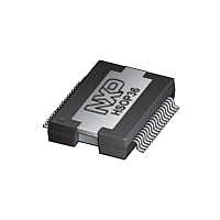
TDF8599A NXP Semiconductors, TDF8599A Datasheet - Page 30

TDF8599A
Manufacturer Part Number
TDF8599A
Description
The TDF8599A is a dual Bridge-Tied Load (BTL) car audio amplifier comprising anNDMOST-NDMOST output stage based on SOI BCDMOS technology
Manufacturer
NXP Semiconductors
Datasheet
1.TDF8599A.pdf
(54 pages)
Available stocks
Company
Part Number
Manufacturer
Quantity
Price
Part Number:
TDF8599ATD
Manufacturer:
NXP/恩智浦
Quantity:
20 000
Part Number:
TDF8599ATH
Manufacturer:
NXP/恩智浦
Quantity:
20 000
NXP Semiconductors
Table 19.
V
[1]
[2]
[3]
[4]
[5]
[6]
[7]
TDF8599A_2
Product data sheet
Symbol
Start-up/shut-down/mute timing
t
t
t
t
t
Speaker load impedance
R
wake
det(DCload)
d(stb-mute)
d(mute-fgain)
d
P
L
= V
Required resistor accuracy for pins ADS and MOD is 1 %; see
Maximum leakage current from DCP pin to ground = 3 A.
The output offset values can be either positive or negative. The V
DC output offset voltage is applied to the output gradually during the transition between Mute mode and Operating mode.
I
The transition time between Mute mode and Operating mode is determined by the time constant on the SEL_MUTE pin.
The DC load valid bit DB1[D6] must be used;
detection cycle to prevent amplifier hang-up incidents.
2
C-bus mode only.
DDA
= 14.4 V; f
Static characteristics
Parameter
wake-up time
DC load detection time
delay time from standby to
mute
mute to full gain delay time
delay time
load resistance
osc
= 320 kHz; 40 C < T
…continued
Section 8.6.2.1 on page
amb
< +85 C; unless otherwise specified.
Rev. 02 — 30 June 2009
Conditions
on pin EN before first I
transmission is recognized
C
measured from amplifier enabling
to start of unmute (no DC load
detection); C
C
C
shutdown delay time from EN pin
LOW to SVRR LOW; voltage on
pin SVRR < 0.1 V; C
shutdown delay time from EN pin
LOW to SVRR LOW; voltage on
pin SVRR < 0.1 V; C
V
shutdown hold delay time from pin
EN LOW to ACGND LOW; voltage
on pin ACGND < 0.1 V; Master
mode
hold delay in Master mode to allow
slaved devices to shutdown
f
at supply voltage equal to or below
25 V
at supply voltage equal to or below
35 V
osc
P
ON
ON
ON
stereo mode
parallel mode
stereo mode
parallel mode
= 35 V
= 320 kHz
I
= 470 nF
= 470 nF
= 470 nF
2
C-bus controlled dual channel class-D power amplifier
Section 9 on page
th(offset)
SVRR
18. The DC load enable bit IB2[D2] must be reset after each load
limit values (excluding Typ) are the valid absolute values.
= 47 F
SVRR
SVRR
2
C-bus
23.
= 47 F
= 47 F;
[5]
[5]
[6]
Min
-
-
-
-
200
300
-
-
1.6
0.8
3.2
1.6
TDF8599A
Typ
-
380
140
15
350
400
370
50
4
-
4
-
© NXP B.V. 2009. All rights reserved.
Max
500
-
-
-
550
700
-
-
-
-
-
-
30 of 54
Unit
ms
ms
ms
ms
ms
ms
ms
s


