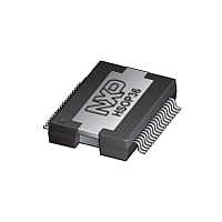
TDF8599A NXP Semiconductors, TDF8599A Datasheet - Page 20

TDF8599A
Manufacturer Part Number
TDF8599A
Description
The TDF8599A is a dual Bridge-Tied Load (BTL) car audio amplifier comprising anNDMOST-NDMOST output stage based on SOI BCDMOS technology
Manufacturer
NXP Semiconductors
Datasheet
1.TDF8599A.pdf
(54 pages)
Available stocks
Company
Part Number
Manufacturer
Quantity
Price
Part Number:
TDF8599ATD
Manufacturer:
NXP/恩智浦
Quantity:
20 000
Part Number:
TDF8599ATH
Manufacturer:
NXP/恩智浦
Quantity:
20 000
NXP Semiconductors
TDF8599A_2
Product data sheet
8.6.2.2 Recommended start-up sequence with DC load detection enabled
Table 12.
Remark: After DC load detection has been performed, the DC load valid bit DB1[D6] must
be set. The DC load data bits are only valid when bit DB1[D6] = 1. When DC load
detection is interrupted by a sudden large change in supply voltage (triggered by UVP or
OVP) or if the amplifier hangs up, the DC load valid bit is reset to DB1[D6] = 0. The DC
load detection enable bit IB2[D2] must be reset after the DC load protection cycle to
release any amplifier hang-up. Once the DC load detection cycle has finished, DC load
detection can be restarted by toggling the DC load detection enable bit IB2[D2]. However,
this can only be used if both amplifier channels have not been enabled with bit IB1[D1] or
bit IB2[D1]. See
detection enabled”
The flow diagram
detection without starting the amplifiers. After a DC load detection cycle finishes without
setting the DC load valid bit DB1[D6], DC load detection is repeated (when bit IB2[D2] is
toggled).
To limit the maximum number of DC load detection cycle loops, a counter and limit have
been added. The loop exits after the predefined number of cycles (COUNTMAX), if the
DC load detection cycle finishes with an invalid detection.
Depending on the application needs, the invalid DC load detection cycle can be handled
as follows:
DC load bits DB1[D4] and DB2[D4]
0
0
1
•
•
the amplifier can be started without DC load detection
the DC load detection loop can be executed again
Interpretation of DC load detection bits
Section 8.6.2.2 “Recommended start-up sequence with DC load
(Figure
for detailed information.
Rev. 02 — 30 June 2009
19) illustrates the TDF8599A’s ability to perform a DC load
I
2
C-bus controlled dual channel class-D power amplifier
OCP bits DB1[D3] and DB2[D3]
0
1
0
TDF8599A
Description
speaker load
shorted load
open load
© NXP B.V. 2009. All rights reserved.
20 of 54


