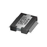
TDF8599A NXP Semiconductors, TDF8599A Datasheet - Page 22

TDF8599A
Manufacturer Part Number
TDF8599A
Description
The TDF8599A is a dual Bridge-Tied Load (BTL) car audio amplifier comprising anNDMOST-NDMOST output stage based on SOI BCDMOS technology
Manufacturer
NXP Semiconductors
Datasheet
1.TDF8599A.pdf
(54 pages)
Available stocks
Company
Part Number
Manufacturer
Quantity
Price
Part Number:
TDF8599ATD
Manufacturer:
NXP/恩智浦
Quantity:
20 000
Part Number:
TDF8599ATH
Manufacturer:
NXP/恩智浦
Quantity:
20 000
NXP Semiconductors
TDF8599A_2
Product data sheet
Fig 20. Start-up and shutdown timing in I
IB1[D0] and
SEL_MUTE
IB2[D0] = 0
(1) Shutdown hold delay.
(2) Master mode shutdown delay.
(3) Shutdown delay.
ACGND
SVRR
OUTn
DIAG
V
DDA
EN
8.6.3 Start-up and shutdown sequence
To prevent switch on or switch off ‘pop noises’, a capacitor (C
SVRR is used to smooth start-up and shutdown. During start-up and shutdown, the output
voltage tracks the voltage on pin SVRR. Increasing C
shutdown time. Enhanced pop noise performance is achieved by muting the amplifier until
the SVRR voltage reaches its final value and the outputs start switching. The capacitor
value on pin SEL_MUTE (C
pin SEL_MUTE determines the amplifier gain. Increasing C
mute times. In addition, a larger C
When the amplifier is switched off with an I
amplifier is first muted and then capacitor (C
In Slave mode, the device enters the off state immediately after capacitor (C
discharged. In Master mode, the clock is kept active by an additional delay (t
approximately 50 ms to allow slave devices to enter the off state.
When an external clock is connected to pin OSCIO (in Slave mode), the clock must
remain active during the shutdown sequence for delay (t
TDF8599A devices are able to enter the off state.
t
wake
t
d(stb-mute)
t
det(DCload)
2
C-bus mode with DC load detection
Rev. 02 — 30 June 2009
t
d(mute-fgain)
ON
I
2
) determines the unmute and mute timing. The voltage on
C-bus controlled dual channel class-D power amplifier
ON
value increases the DC load detection cycle.
t
d
2
(3)
C-bus command or by pulling pin EN LOW, the
SVRR
) is discharged.
SVRR
d
(1)
results in a longer start-up and
) to ensure that the slaved
ON
SVRR
increases the unmute and
) connected to pin
TDF8599A
mute delay
© NXP B.V. 2009. All rights reserved.
t
d
(1)
t
SVRR
d
d
(2)
(2)
) of
001aai790
) is
22 of 54


