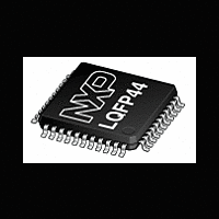
XA-C3 NXP Semiconductors, XA-C3 Datasheet - Page 14

XA-C3
Manufacturer Part Number
XA-C3
Description
The XA-C3 is a member of the Philips XA (eXtended Architecture) family of high-performance 16-bit single-chip microcontrollers
Manufacturer
NXP Semiconductors
Datasheet
1.XA-C3.pdf
(68 pages)
Philips Semiconductors
PIN DESCRIPTIONS
Table 4. Pin Descriptions
2000 Jan 25
XA 16-bit microcontroller family
32K/1024 OTP CAN transport layer controller
1 UART, 1 SPI Port, CAN 2.0B, 32 CAN ID filters, transport layer co-processor
MNEMONIC
P0.0 – P0.7
P1.0 – P1.7
P2.0 – P2.7
P3.0 – P3.7
P1.0
P1.1
P1.2
P1.3
P1.4
P1.5
P1.6
P1.7
P3.0
P3.1
P3.2
P3.3
V
V
SS
DD
43 – 36
24 – 31
13 – 19
PLCC
23, 44
1, 22
2 – 9
PIN NUMBERS
11,
11
13
14
15
2
3
4
5
6
7
8
9
40 – 44
18 – 25
16, 39
17, 38
37–30
LQFP
7 –12
1 – 3
40
41
42
43
44
5,
1
2
3
5
7
8
9
TYPE
I/O
I/O
I/O
I/O
O
O
O
O
O
O
O
I
I
I
I
I
I
I
Ground: 0V Reference.
Power Supply: This is the power supply voltage for normal, Idle and Power–Down op-
eration.
Port 0: Port 0 is an 8–bit I/O Port with user –configurable pins. Port 0 latches have 1’s
written to them and are configured in the Quasi–Bidirectional mode during Reset. The
operation of Port 0 pins as inputs or outputs depends upon the Port configuration se-
lected. Each Port pin is configured independently. Refer to the sections on I/O Port
configuration and DC Electrical Characteristics for details.
NOTE:
2. When the External PROGRAM/DATA bus is used, Port 0 becomes the multiplexed
Port 1: Port 1 is an 8–bit I/O Port with user –configurable pins. Port 1 latches have 1’s
written to them and are configured in the Quasi–Bidirectional mode during Reset. The
operation of Port 1 pins as inputs or outputs depends upon the Port configuration se-
lected. Each Port pin is configured independently. Refer to the sections on I/O Port
configuration and DC Electrical Characteristics for details.
WRH/: Address bit 0 of the External Address bus when the External DATA bus is config-
ured for 8–bit width. When the External DATA bus is used, this pin becomes the High
Byte Write Strobe (WRH).
A1:
A2:
A3:
SPIRx: Receiver serial input of SPI.
SPITx: Transmitter serial output of SPI.
T2 ; SPICLK: Timer/counter 2 external clock input or Timer/counter 2 Clock–Out mode
output, or SPI Clock output.
NOTES:
3. SPICLK must be configured to idle in the logic ‘1’ state in order to use either the T2
4. The default state from Reset of the SPICLK polarity is “inverted” which yields an
5. If the SPI Clock polarity is changed by the user during SPI Port usage, it must be
T2EX: Timer/counter 2 reload/capture/direction control.
Port 2: Port 2 is an 8–bit I/O port with user–configurable pins. Port 2 latches have 1’s
written to them and are configured in the Quasi–Bidirectional mode during Reset. The
operation of Port 2 pins as inputs or outputs depends upon the Port configuration se-
lected. Each Port pin is configured independently.
Refer to the sections on I/O port configuration and DC Electrical Characteristics for de-
tails.
NOTES:
6. When the External 16–bit PROGRAM/DATA bus is used, Port 2 is MUXed between
Port 3: Port 3 is an 8–bit I/O Port with user–configurable pins.
NOTES:
7. Port 3 latches have 1’s written to them and are configured in the Quasi–Bidirectional
8. The operation of Port 3 pins as inputs or outputs depends upon the Port
9. Each Port pin is configured independently.
Refer to the sections on I/O Port configuration and DC Electrical Characteristics for
details.
RxD0: Receiver serial input of UART 0.
TxD0: Transmitter serial output of UART 0.
INT0/: External interrupt 0 input.
INT1/: External interrupt 1 input.
low DATA/Instruction Byte and Address lines 4 through 11.
or P1.6 output functions, even if the SPI Port is not in use!
SPICLK idle state of logic ‘1’.
restored to “inverted” polarity before using either the P1.6 or Timer/counter 2 output
functions.
High (DATA/Instruction) Byte and Address lines 12 through 19.
mode during Reset.
configuration selected.
Address bit 1 of the External Address bus.
Address bit 2 of the External Address bus.
Address bit 3 of the External Address bus.
7
NAME AND FUNCTION
Preliminary specification
XA-C3


