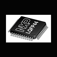
XA-C3 NXP Semiconductors, XA-C3 Datasheet - Page 62

XA-C3
Manufacturer Part Number
XA-C3
Description
The XA-C3 is a member of the Philips XA (eXtended Architecture) family of high-performance 16-bit single-chip microcontrollers
Manufacturer
NXP Semiconductors
Datasheet
1.XA-C3.pdf
(68 pages)
- Current page: 62 of 68
- Download datasheet (369Kb)
Philips Semiconductors
Special Function Register MRBH
MRBH
Special Function Register MRBL
MRBL
MRBE
On–Chip Message Buffer RAM (XRAM)
The XA-C3 has a 512–byte on–chip message buffer RAM (XRAM)
which may contain part or all of the CAN/CTL (transmit & receive
objects) message buffers. This block of memory can be accessed
as regular data memory. The logic address of the XRAM is
programmed by software, and must start at a 512–Byte boundary.
The base address of the XRAM is determined by the contents of
Memory Mapped Registers MBXSR and XRAMB as shown in and .
Any address asserted by the XA core (or the DMA) whose fifteen
most significant bits match the concatenation
2000 Jan 25
Address: SFR 497h
Address: SFR 496h
XA 16-bit microcontroller family
32K/1024 OTP CAN transport layer controller
1 UART, 1 SPI Port, CAN 2.0B, 32 CAN ID filters, transport layer co-processor
7
7
a15 – a12 of MMR Base Address
MRBE is the global enable bit for MMRs. On
reset, MRBE is cleared to 0.
0 = MMRs disabled
1 = MMRs enabled
6
6
Figure 44. Detail of MMR space showing block of Message Object Registers
Offset FFFh
Offset 1FFh
5
5
a23 – a16 of MMR Base Address
512 Bytes Object Registers
4
4
MMR Space
55
MBXSR[7:0]XRAMB[7:1] will be automatically routed to the XRAM.
On reset, the XRAM is disabled. Note: The XRAM should not be
confused with the 1K Byte “scratch–pad” DATA RAM which is also
provided on–chip .
Since the uppermost 8 bits of all message buffer addresses are
formed by the contents of the MBXSR register, the XRAM and all 32
message buffers must reside in the same 64K byte data memory
segment. Since the XA-C3 only provides address lines A1 – A19 for
accessing External memory, all External memory addresses must
be within the lowest 1M byte of address space. Therefore, if there is
External memory in the system into which any of the 32 message
buffers will be mapped, then all 32 message buffers and the XRAM
must also be mapped entirely into that same 64K byte segment,
which must be below the 1M byte address limit.
Reset Value: 0Fh
Reset Value: F0h
3
3
–
Offset 000h
2
2
–
SU01341
1
1
–
Preliminary specification
XA-C3
MRBE
0
0
Related parts for XA-C3
Image
Part Number
Description
Manufacturer
Datasheet
Request
R

Part Number:
Description:
IC XA MCU 16BIT 32K OTP 44-PLCC
Manufacturer:
NXP Semiconductors
Datasheet:

Part Number:
Description:
IC XA MCU 16BIT 32K OTP 80-LQFP
Manufacturer:
NXP Semiconductors
Datasheet:

Part Number:
Description:
IC XA MCU 16BIT 32K OTP 68-PLCC
Manufacturer:
NXP Semiconductors
Datasheet:

Part Number:
Description:
IC XA MCU 16BIT ROMLESS 68-PLCC
Manufacturer:
NXP Semiconductors
Datasheet:

Part Number:
Description:
IC XA MCU 16BIT ROMLESS 44-PLCC
Manufacturer:
NXP Semiconductors
Datasheet:

Part Number:
Description:
IC XA MCU 16BIT 32K OTP 68-PLCC
Manufacturer:
NXP Semiconductors
Datasheet:

Part Number:
Description:
IC XA MCU 16BIT ROMLESS 44-LQFP
Manufacturer:
NXP Semiconductors
Datasheet:

Part Number:
Description:
IC XA MCU 16BIT 32K OTP 44-PLCC
Manufacturer:
NXP Semiconductors
Datasheet:

Part Number:
Description:
IC XA MCU 16BIT FLASH 64K 44PLCC
Manufacturer:
NXP Semiconductors
Datasheet:

Part Number:
Description:
IC XA MCU 16BIT FLASH 64K 44PLCC
Manufacturer:
NXP Semiconductors
Datasheet:

Part Number:
Description:
IC XA MCU 16BIT ROMLESS 44-PLCC
Manufacturer:
NXP Semiconductors
Datasheet:

Part Number:
Description:
IC XA MCU 16BIT ROMLESS 44-PLCC
Manufacturer:
NXP Semiconductors
Datasheet:

Part Number:
Description:
IC XA MCU 16BIT FLASH 64K 44LQFP
Manufacturer:
NXP Semiconductors
Datasheet:

Part Number:
Description:
IC XA MCU 16BIT 32K OTP 44-PLCC
Manufacturer:
NXP Semiconductors
Datasheet:
Part Number:
Description:
IC XA MCU 16BIT CMOS 100LQFP
Manufacturer:
NXP Semiconductors
Datasheet:


