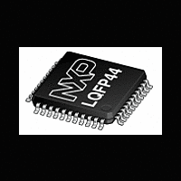
XA-C3 NXP Semiconductors, XA-C3 Datasheet - Page 48

XA-C3
Manufacturer Part Number
XA-C3
Description
The XA-C3 is a member of the Philips XA (eXtended Architecture) family of high-performance 16-bit single-chip microcontrollers
Manufacturer
NXP Semiconductors
Datasheet
1.XA-C3.pdf
(68 pages)
Philips Semiconductors
MNMSKL
MnCTL: Message n Control Register
MNCTL
OBJ_EN
INT_EN
Tx/Rx
FRAG
MBXSR
All 32 message buffers must reside within the same 64K memory
page. This page is specified by the contents of the MBXSR
(Message Buffer and XRAM Segment Register) register. Also, the
512 byte on–chip message buffer RAM (XRAM) is always positioned
within that same 64K page pointed to by MBXSR.
Note: The XA-C3 brings out only 20 address lines to package pins.
It can, therefore, only address 1MByte of off–chip data memory (a
maximum of sixteen 64K segments). As a result, for the XA-C3, the
MNBSZ
The size of an object’s message buffer is specified with the 3–bit
field MnBSZ[2:0] as shown in Table 23.
2000 Jan 25
Msk12
Address: MMR base + n8h
XA 16-bit microcontroller family
32K/1024 OTP CAN transport layer controller
1 UART, 1 SPI Port, CAN 2.0B, 32 CAN ID filters, transport layer co-processor
15
7
–
7
7
–
Msk11
14
Object Enable. Enables the Message Object for
receive or transmit. 0 = disabled, 1 = enabled.
Message–Complete Interrupt Enable. Specifies
whether or not a Tx or Rx Message–Complete
for this object will cause the object’s
Message–Complete Interrupt to be generated. 0
= disabled, 1 = enabled.
Transmit or Receive. Specifies whether this is a
transmit or receive Message Object. 0 =
transmit object, 1 = receive object.
Fragmented Message Enable. Only relevant for
receive Message Objects. Enables automatic
assembly of Fragmented Rx messages. If
disabled, messages received by this object are
assumed to be single–frame, or will be
assembled by User software. 0 = disabled, 1 =
enabled. Note: Masking of the CAN Identifier
field by User software, for the purpose of
Message Object grouping, is disallowed for
objects using hardware Fragmentation
assembly. However, Masking of unused bit
positions in the “screener”, such is mandatory in
all cases.
Msk10
13
6
–
6
6
–
Msk9
12
a23 – a16 of all message buffer (and XRAM) base addresses
Msk8
11
5
–
5
5
–
Msk7
10
OBJ_EN
Msk6
9
4
4
4
–
Msk5
8
41
RTR_EN
Message Storage
When an incoming message frame has passed acceptance filtering,
it will be automatically stored in data memory via DMA. Each
message will be stored in its corresponding buffer area. On setup,
the User is responsible for assigning a unique buffer location for
each Message Object. This is specified in the object’s MnBLR
register. The User is also required to set up the size of each buffer in
the MnBSZ register.
The XA-C3 provides a total of 512 bytes of on–chip message buffer
RAM (XRAM) which may contain part or all of the CAN/CTL
(transmit & receive) message buffer space. See Section entitled
On-Chip Message Buffer RAM (XRAM) on page 55 for details.
Note: The following discussion concerning message buffer registers
applies to transmit message retrieval as well as receive message
storage.
MBXSR (applies to all objects)
four most significant bits of the MBSXR register must be set to
‘0000’ if External RAM is to be used for any portion of the message
buffer space.
MnBSZ: Message n Buffer Size Register
INT_EN
Msk4
Access: Read, write. Byte or word access.
Reset value: 00000xxxb (unused bits are always read as ‘0’)
Address: MMR base + 291h
Access: Read, write, byte or word
Reset value: FFh
Address: MMR base + nCh
Access: Read–modify–write, byte or word access.
Reset value: 00000xxxb
7
3
3
3
–
Msk3
6
Msk2
BSZ.2
Tx/Rx
Enable Request To Transmit. 0 = the object is
not enabled for RTR handling, 1 = the object is
enabled for RTR handling. See section entitled
RTR Handling , page 46.
5
2
2
2
Msk1
4
Msk0
FRAG
BSZ.1
3
1
1
1
Preliminary specification
2
–
XA-C3
RTR_EN
1
–
BSZ.0
0
0
0
0
–


