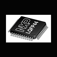
XA-C3 NXP Semiconductors, XA-C3 Datasheet - Page 35

XA-C3
Manufacturer Part Number
XA-C3
Description
The XA-C3 is a member of the Philips XA (eXtended Architecture) family of high-performance 16-bit single-chip microcontrollers
Manufacturer
NXP Semiconductors
Datasheet
1.XA-C3.pdf
(68 pages)
1. Load capacitance for all outputs = 80pF.
2. Variables V1 through V13 reflect programmable bus timing, which is
Philips Semiconductors
AC ELECTRICAL CHARACTERISTICS
Table 20. AC Electrical Characteristics
V
NOTES:
2000 Jan 25
SYMBOL
External Clock
f
t
t
t
t
t
Address Cycle
t
t
t
t
Code Read Cycle
t
t
t
t
t
t
t
t
Data Read Cycle
t
t
t
t
t
t
t
t
Data Write Cycle
t
t
t
t
t
t
WAIT Input
t
t
DD
C
C
CHCX
CLCX
CLCH
CHCL
CRAR
LHLL
AVLL
LLAX
PLPH
LLPL
AVIVA
AVIVB
PLIV
PXIX
PXIZ
IXUA
RLRH
LLRL
AVDVA
AVDVB
RLDV
RHDX
RHDZ
DXUA
WLWH
LLWL
QVWX
WHQX
AVWL
UAWH
WTH
WTL
XA 16-bit microcontroller family
32K/1024 OTP CAN transport layer controller
1 UART, 1 SPI Port, CAN 2.0B, 32 CAN ID filters, transport layer co-processor
programmed via the Bus Timing registers (BTRH and BTRL).
Refer to the XA User Guide for details of the bus timing settings.
V1)
V2)
= 4.5V to 5.5V; T
This variable represents the programmed width of the ALE pulse
as determined by the ALEW bit in the BTRL register.
V1 = 0.5 if the ALEW bit = 0, and 1.5 if the ALEW bit = 1.
This variable represents the programmed width of the PSEN/ pulse
as determined by the CR1 and CR0 bits or the CRA1, CRA0, and
ALEW bits in the BTRL register.
–
For a bus cycle with no ALE, V2 = 1 if CR1/0 = 00, 2 if CR1/0
= 01, 3 if CR1/0 = 10, and 4 if CR1/0 = 11. Note that during
burst mode code fetches, PSEN/ does not exhibit transitions at
Figure
22
22
22
22
22
21
16
16
16
16
16
16
17
16
16
16
16
18
18
18
19
18
18
18
18
20
20
20
20
20
20
21
21
amb
= 0 to +70 C for commercial, –40 C to +85 C for industrial.
PARAMETER
Oscillator frequency
Clock period and CPU timing cycle
Clock high time
Clock low time
Clock rise time
Clock fall time
Delay from clock rising edge to ALE rising edge
ALE pulse width (programmable)
Address valid to ALE de–asserted (set–up)
Address hold after ALE de–asserted
PSEN/ pulse width
ALE de–asserted to PSEN/ asserted
Address valid to instruction valid, ALE cycle (access time)
Address valid to instruction valid, non–ALE cycle (access time)
PSEN/ asserted to instruction valid (enable time)
Instruction hold after PSEN/ de–asserted
Bus 3–State after PSEN/ de–asserted (disable time)
Hold time of unlatched part of address after instruction latched
RD/ pulse width
ALE de–asserted to RD/ asserted
Address valid to data input valid, ALE cycle (access time)
Address valid to data input valid, non–ALE cycle (access time)
RD/ low to valid data in, enable time
Data hold time after RD/ de–asserted
Bus 3–State after RD/ de–asserted (disable time)
Hold time of unlatched part of address after data latched
WR/ pulse width
ALE falling edge to WR/ asserted
Data valid before WR/ asserted (data setup time)
Data hold time after WR/ de–asserted (Note 6)
Address valid to WR/ asserted (address setup time) (Note 5)
Hold time of unlatched part of address after WR/ is de–asserted
WAIT stable after bus strobe (RD/, WR/, or PSEN/) asserted
WAIT hold after bus strobe (RD/, WR/, or PSEN/) assertion
28
V3)
–
This variable represents the programmed length of an entire code
read cycle with ALE. This time is determined by the CRA1 and
CRA0 bits in the BTRL register. V3 = the total bus cycle duration (2
if CRA1/0 = 00, 3 if CRA1/0 = 01, 4 if CRA1/0 = 10,
and 5 if CRA1/0 = 11).
the boundaries of bus cycles. V2 still applies for the purpose of
determining peripheral timing requirements.
For a bus cycle with an ALE, V2 = the total bus cycle duration
(2 if CRA1/0 = 00, 3 if CRA1/0 = 01, 4 if CRA1/0 = 10,
and 5 if CRA1/0 = 11) minus the number of clocks used by
ALE (V1 + 0.5).
Example: If CRA1/0 = 10 and ALEW = 1, the V2 = 4 – (1.5 +
0.5) = 2.
MIN
0
1/f
t
t
10
(V1 * t
(V1 * t
(t
(V2 * t
(t
0
0
(V7 * t
(t
0
0
(V8 * t
(V12 * t
(V13 * t
(V11 * t
(V9 * t
(V11 * t
(V10 * t
C
C
C
C
C
C
* 0.5
* 0.4
/2) – 10
/2) – 7
/2) – 7
C
C
C
C
C
C
C
C
) – 6
) – 12
) – 10
) – 10
) – 10
C
C
) – 22
C
VARIABLE CLOCK
) – 5
) – 7
) – 10
) – 22
) – 5
MAX
32
5
5
46
(V3 * t
(V4 * t
(V2 * t
t
(V6 * t
(V5 * t
(V7 * t
t
(V10 * t
C
C
– 8
– 8
Preliminary specification
C
C
C
C
C
C
) – 36
) – 29
) – 29
) – 36
) – 29
) – 29
C
) – 30
XA-C3
UNIT
MHz
ns
ns
ns
ns
ns
ns
ns
ns
ns
ns
ns
ns
ns
ns
ns
ns
ns
ns
ns
ns
ns
ns
ns
ns
ns
ns
ns
ns
ns
ns
ns
ns
ns


