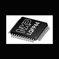
XA-C3 NXP Semiconductors, XA-C3 Datasheet - Page 17

XA-C3
Manufacturer Part Number
XA-C3
Description
The XA-C3 is a member of the Philips XA (eXtended Architecture) family of high-performance 16-bit single-chip microcontrollers
Manufacturer
NXP Semiconductors
Datasheet
1.XA-C3.pdf
(68 pages)
1. Users should never write to the BCR register.
2. Users must ALWAYS INITIALIZE (Write) 00h to this register.
3. Port configurations default to Quasi–Bidirectional when the XA begins execution from Internal code memory after Reset, based on the
4. SFR is loaded from the Reset vector.
5. All bits except F1, F0, and P are loaded from the Reset vector. Those bits are all 0.
6. The WDCON Reset value is E6h for a Watchdog Reset, E4h for all other Reset causes. The Watchdog is always turned ON as one
Philips Semiconductors
NOTES:
GENERAL NOTES:
– SFRs marked with an asterisk (*) are bit–addressable.
– The XA–C3 implements an 8–bit SFR bus, as stated in Chapter 8 of the XA User Guide . All SFR accesses must be 8–bit operations.
– Unimplemented bits in SFRs (indicated by ”–”} are unknown at all times. Ones should not be written to these bits since they may be used for
– The XA guards writes to all SFR bits that can be modified by hardware, including all SFR resident interrupt flags, as well as the WDTOF bit in
2000 Jan 25
S0STAT*
S0BUF
S0ADDR
S0ADEN
SCR
SSEL*
SWE
SWR*
T2CON*
T2MOD*
TH2
TL2
T2CAPH
T2CAPL
TCON*
TH0
TH1
TL0
TL1
TMOD
TSTAT*
WDCON*
WDL
WFEED1
WFEED2
Attempts to write 16 bits to an SFR will actually write only the lower 8 bits. Sixteen–bit SFR reads will return undefined data in the upper byte.
other purposes in future XA derivatives. In general, the Reset value shown for these unimplemented bits is 00h.
WDCON. This mechanism, called Read–Modify–Write Lockout, prevents loss of an interrupt (or other status) flag if a bit is written to directly
by hardware between the read and write of an instruction that performs a read–modify–write operation.
NAME
XA 16-bit microcontroller family
32K/1024 OTP CAN transport layer controller
1 UART, 1 SPI Port, CAN 2.0B, 32 CAN ID filters, transport layer co-processor
condition found on the EA
execution using External code memory, the default configuration for pins that are associated with the External bus will be Push–Pull. The
PnCFGA and PnCFGB register contents will reflect this difference.
consequence of RST/. Therefore, the user should turn OFF the Watchdog if immediate Watchdog operation is not desired: See the
Watchdog Timer section in this Data Sheet for a recommended code example.
Serial port 0 extended status
Serial port 0 buffer register
Serial port 0 address register
Serial port 0 address enable
register
System configuration register
Segment selection register
Software Interrupt Enable
Software Interrupt Request
Timer 2 control register
Timer 2 mode control
Timer 2 high byte
Timer 2 low byte
Timer 2 capture register, high
byte
Timer 2 capture register, low
byte
Timer 0 and 1 control register
Timer 0 high byte
Timer 1 high byte
Timer 0 low byte
Timer 1 low byte
Timer 0 and 1 mode control
Timer 0 and 1 extended status
Watchdog control register
Watchdog timer reload
Watchdog feed 1
Watchdog feed 2
DESCRIPTION
/
pin. Thus, all PnCFGA registers will contain FFh and PnCFGB registers will contain 00h. When the XA begins
ADDRESS
47Ah
42Ah
45Bh
45Ah
45Ch
45Dh
45Eh
421h
460h
461h
462h
440h
403h
418h
419h
459h
458h
410h
451h
453h
450h
452h
411h
41Fh
45Fh
SFR
GATE1
ESWEN
PRE2
2C7
2CF
30F
21F
357
TF2
287
TF1
28F
2FF
–
–
–
–
–
–
7
C1 or T1/
R6SEG
SWE7
SWR7
EXF2
PRE1
2C6
2CE
TR1
2FE
30E
21E
356
286
28E
6
–
–
–
–
10
BIT FUNCTIONS AND BIT ADDRESSES
R5SEG
RCLK0
SWR6
SWE6
PRE0
2CD
30D
21D
2C5
28D
2FD
355
285
TF0
M1
–
–
–
–
5
R4SEG
TCLK0
SWR5
SWE5
30C
21C
2C4
2CC
TR0
28C
2FC
354
284
M0
4
–
–
–
–
–
R3SEG
EXEN2
GATE0
SWR4
SWE4
30B
FE0
PT1
21B
2C3
2CB
28B
2FB
353
283
IE1
3
–
–
–
C0 or T0/
WDRUN
R2SEG
SWE3
SWR3
T1OE
BR0
2CA
30A
PT0
21A
2C2
TR2
28A
2FA
352
282
IT1
2
–
WDTOF
R1SEG
SWE2
SWR2
T2OE
C2 or
OE0
2C1
2C9
2F9
309
CM
219
351
281
IE0
289
T2/
M1
1
–
Preliminary specification
STINT0
R0SEG
SWR1
SWE1
DCEN
CP or
T0OE
RL2/
2C0
2C8
308
218
350
280
288
2F8
IT0
M0
PZ
0
–
00h
xxh
00h
00h
00h
00h
00h
00h
00h
00h
00h
00h
00h
00h
00h
00h
00h
00h
00h
00h
00h
Note 6
00h
xxh
xxh
XA-C3
RESET
VALUE


