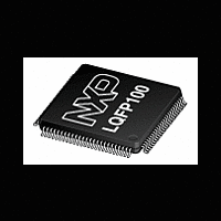
XA-H4 NXP Semiconductors, XA-H4 Datasheet - Page 21

XA-H4
Manufacturer Part Number
XA-H4
Description
The powerful 16-bit XA CPU core and rich feature set make the XA-H3 and XA-H4 devices ideal for high-performance real-time applications such as industrial control and networking
Manufacturer
NXP Semiconductors
Datasheet
1.XA-H4.pdf
(42 pages)
Philips Semiconductors
Clock Output
The ClkOut pin allows easier external bus interfacing in some
situations. This output reflects the XTALIn clock input to the XA
(referred to internally as CClk or System Clock), but is delayed to
match the external bus outputs and strobes. The default is for
1999 Sep 24
Single-chip 16-bit microcontroller
NOTE:
The 16-bit wide RAM does not need the A0 pin from the processor. During byte writes to the RAM, the A0 value will cause
either BLE or BHE pin to go active from the XA-H3, but not to both. For all Word Writes, Word Reads, Code Fetches, and
Byte Reads, both BLE and BHE will go active.During DRAM cycles only, the appropriate CAS Address will be multiplexed
onto pins A17 – A7 after the assertion of RAS and prior to the assertion of BHE (CASH) and BLE (CASL.) See AC timing
diagrams and the XA-H4 User Manual for complete details.
XA-H4
D15–D0
A19–A0
BHE
CS0
CS1
CS2
CS3
BLE
WE
OE
Figure 4. Typical system bus configuration
21
ClkOut to be output enabled at reset, but it may be turned off
(tri-state disabled) by software via the MICFG MMR.
WARNING: The capacitive loading on this output must not
exceed 40 pf.
A16–A0
A17–A9
D15–D0
A17–A8
D15–D0
A15–A1
D15–D0
D7–D0
CS
OE
A16–A0
D7–D0
RAS
CASL
CASH
OE
WE
A8–A0
D15–D0
RAS
CASL
CASH
OE
WE
A9–A0
D15–D0
RAS
CASL
CASH
WE
A15–A1
D15–D0
256 k x 16 DRAM
(MT4C1M16C3)
32 k x 16 SRAM
1 M x 16 DRAM
128 k x 8 ROM
(HM514260DI)
Preliminary specification
XA-H4
SU01275


