BLM6G10-30 NXP Semiconductors, BLM6G10-30 Datasheet
BLM6G10-30
Available stocks


Related parts for BLM6G10-30


BLM6G10-30 Summary of contents
Page 1
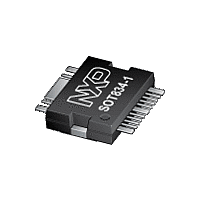
... BLM6G10-30; BLM6G10-30G W-CDMA 860 MHz - 960 MHz power MMIC Rev. 2 — 1 March 2011 1. Product profile 1.1 General description 30 W LDMOS 2-stage power MMIC for base station applications at frequencies from 860 MHz to 960 MHz. Available in Gull Wing for surface mount (SOT822-1) or flat lead (SOT834-1) ...
Page 2
... NXP Semiconductors 2. Pinning information 2.1 Pinning Fig 1. 2.2 Pin description Table 2. Pin 1, 11 flange BLM6G10-30_BLM6G10-30G Product data sheet BLM6G10-30; BLM6G10-30G BLM6G10-30 BLM6G10-30G GND DS1 3 n.c. 4 n. input 7 n. GS1 9 V GS2 V 10 DS1 GND 11 Transparent top view ...
Page 3
... V DS1 6 RF_input 8 V GS1 TEMPERATURE 9 COMPENSATED BIAS V GS2 Block diagram of BLM6G10-30 and BLM6G10-30G Limiting values Parameter drain-source voltage gate-source voltage first stage drain current second stage drain current storage temperature junction temperature Thermal characteristics Parameter first stage thermal resistance from junction to case ...
Page 4
... Symbol Parameter P L(AV D IMD3 ACPR 8. Application information 8.1 Ruggedness The BLMG10-30 and BLM6G10-30G are capable of withstanding a load mismatch corresponding to VSWR = through all phases under the following conditions 8.2 Impedance information Table 7. f MHz 850 860 880 900 920 ...
Page 5
... NXP Semiconductors 8.3 Performance curves Performance curves are measured in a BLM6G10-30G application circuit (dB) 33 η 880 920 = 25 case 288 mA; carrier spacing = 10 MHz. Dq2 Fig 3. 2-carrier W-CDMA power gain and drain efficiency as function of frequency; typical values ...
Page 6
... CCDF. = 30 C (1) T case = 25 C (2) T case = 80 C (3) T case Fig 9. Single-carrier peak output power (peaks 3 dB compressed) as function of frequency and temperature; typical values BLM6G10-30_BLM6G10-30G Product data sheet BLM6G10-30; BLM6G10-30G 001aak505 IMD (dBc (W) L Fig L(M) (W) ...
Page 7
... NXP Semiconductors 8.4 Application circuit Fig 10. Class-AB application circuit BLM6G10-30_BLM6G10-30G Product data sheet BLM6G10-30; BLM6G10-30G W-CDMA 860 MHz - 960 MHz power MMIC BLM6G1030 BOARD 3 DEV REV1 All information provided in this document is subject to legal disclaimers. Rev. 2 — 1 March 2011 001aan772 © NXP B.V. 2011. All rights reserved. ...
Page 8
... Printed-Circuit Board (PCB): Rogers 4350B; metallization). Component C1, C2, C5, C13, C16 C3, C4, C14, C17 C6, C12, C15 C7 C8, C9 C10, C11 C18 R1 R2 [1] American Technical Ceramics type 100A or capacitor of same quality. BLM6G10-30_BLM6G10-30G Product data sheet BLM6G10-30; BLM6G10-30G V C7 DS1 GS1 GS2 ...
Page 9
... For test circuit see Component C1, C2, C13, C14 C3, C4, C5, C11, C12 C6, C9, C10 C7, C8 C15 C16 C17, C18 [1] American Technical Ceramics type 100A or capacitor of same quality. BLM6G10-30_BLM6G10-30G Product data sheet BLM6G10-30; BLM6G10-30G C17 V DS1 GS1 GS2 V BLM6G1030 ...
Page 10
... Note 1. Plastic or metal protrusions of 0.25 mm maximum per side are not included. Outline version IEC SOT834-1 Fig 13. Package outline SOT834-1 BLM6G10-30_BLM6G10-30G Product data sheet BLM6G10-30; BLM6G10-30G (2× (5×) e (2× (10× ...
Page 11
... Note 1. Plastic or metal protrusions of 0.25 mm maximum per side are not included Outline version IEC SOT822-1 Fig 14. Package outline SOT822-1 BLM6G10-30_BLM6G10-30G Product data sheet BLM6G10-30; BLM6G10-30G (2× (2×) b (5× ...
Page 12
... MMIC PA PAR PDPCH RF SMD VSWR W-CDMA 13. Revision history Table 12. Revision history Document ID BLM6G10-30_BLM6G10-30G v.2 20110301 Modifications: BLM6G10-30_BLM6G10-30G v.1 20090828 BLM6G10-30_BLM6G10-30G Product data sheet BLM6G10-30; BLM6G10-30G Moisture sensitivity level Abbreviations Description Third Generation Partnership Project Complementary Cumulative Distribution Function Continuous Wave Dedicated Physical CHannel ...
Page 13
... BLM6G10-30_BLM6G10-30G Product data sheet BLM6G10-30; BLM6G10-30G [3] Definition This document contains data from the objective specification for product development. This document contains data from the preliminary specification. ...
Page 14
... For sales office addresses, please send an email to: BLM6G10-30_BLM6G10-30G Product data sheet BLM6G10-30; BLM6G10-30G NXP Semiconductors’ specifications such use shall be solely at customer’s own risk, and (c) customer fully indemnifies NXP Semiconductors for any liability, damages or failed product claims resulting from customer design and use of the product for automotive applications beyond NXP Semiconductors’ ...
Page 15
... Please be aware that important notices concerning this document and the product(s) described herein, have been included in section ‘Legal information’. © NXP B.V. 2011. For more information, please visit: http://www.nxp.com For sales office addresses, please send an email to: salesaddresses@nxp.com Document identifier: BLM6G10-30_BLM6G10-30G All rights reserved. Date of release: 1 March 2011 ...