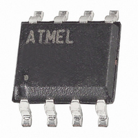
AT45DB161D-SU Atmel, AT45DB161D-SU Datasheet - Page 18

AT45DB161D-SU
Manufacturer Part Number
AT45DB161D-SU
Description
IC FLASH 16MBIT 66MHZ 8SOIC
Manufacturer
Atmel
Datasheets
1.AT45DB161D-CU.pdf
(51 pages)
2.AT45DB161D-SU.pdf
(6 pages)
3.AT45DB161D-SU.pdf
(53 pages)
Specifications of AT45DB161D-SU
Format - Memory
FLASH
Memory Type
DataFLASH
Memory Size
16M (4096 pages x 528 bytes)
Speed
66MHz
Interface
SPI, 3-Wire Serial
Voltage - Supply
2.7 V ~ 3.6 V
Operating Temperature
-40°C ~ 85°C
Package / Case
8-SOIC (5.3mm Width), 8-SOP, 8-SOEIAJ
Architecture
Sectored
Interface Type
SPI
Supply Voltage (max)
3.6 V
Supply Voltage (min)
2.7 V
Maximum Operating Current
15 mA
Mounting Style
SMD/SMT
Organization
128 KB x 16
Current, Input, Leakage
1 μA
Current, Operating
11 mA (Read), 12 mA (Program/Erase)
Current, Output, Leakage
1
Data Retention
20 yrs.
Density
16M
Package Type
EIAJ SOIC
Temperature, Operating
-40 to +85 °C
Time, Access
6 ns
Time, Address Hold
5
Time, Address Setup
5
Time, Fall
6.8 ns
Time, Rise
6.8 ns
Voltage, Input, High
1.89 to 2.52 V
Voltage, Input, Low
0.81 to 1.08 V
Voltage, Output, High
2.5 V
Voltage, Output, Low
0.4 V
Voltage, Supply
2.7 to 3.6 V
Memory Configuration
4096 Pages X 528 Bytes
Clock Frequency
66MHz
Supply Voltage Range
2.5V To 3.6V, 2.7V To 3.6V
Rohs Compliant
Yes
Access Time (max)
6ns
Boot Type
Not Required
Address Bus
1b
Operating Supply Voltage (typ)
3/3.3V
Operating Temp Range
-40C to 85C
Program/erase Volt (typ)
2.7 to 3.6V
Sync/async
Synchronous
Operating Temperature Classification
Industrial
Operating Supply Voltage (min)
2.7V
Operating Supply Voltage (max)
3.6V
Supply Current
15mA
Mounting
Surface Mount
Pin Count
8
Lead Free Status / RoHS Status
Lead free / RoHS Compliant
Available stocks
Company
Part Number
Manufacturer
Quantity
Price
Company:
Part Number:
AT45DB161D-SU
Manufacturer:
ATMEL
Quantity:
106 020
Company:
Part Number:
AT45DB161D-SU
Manufacturer:
AYMEL
Quantity:
1
Part Number:
AT45DB161D-SU
Manufacturer:
ATMEL/爱特梅尔
Quantity:
20 000
Part Number:
AT45DB161D-SU-2.5
Manufacturer:
ATMEL/爱特梅尔
Quantity:
20 000
Company:
Part Number:
AT45DB161D-SU-N03
Manufacturer:
NS
Quantity:
487
Company:
Part Number:
AT45DB161D-SU-SL383
Manufacturer:
AMS
Quantity:
30 000
10.2
10.2.1 Programming the Security Register
18
Security Register
The device contains a specialized Security Register that can be used for purposes such as unique device
serialization or locked key storage. The register is comprised of a total of 128-bytes that is divided into two
portions. The first 64-bytes (byte locations 0 through 63) of the Security Register are allocated as a one-time user
programmable space. Once these 64-bytes have been programmed, they cannot be reprogrammed. The
remaining 64-bytes of the register (byte locations 64 through 127) are factory programmed by Atmel
contain a unique value for each device. The factory programmed data is fixed and cannot be changed.
Table 10-5.
The user programmable portion of the Security Register does not need to be erased before it is programmed.
To program the Security Register, the CS pin must first be asserted and the appropriate 4-byte opcode sequence
must be clocked into the device in the correct order. The 4-byte opcode sequence must start with 9BH and be
followed by 00H, 00H, and 00H. After the last bit of the opcode sequence has been clocked into the device, the
data for the contents of the 64-byte user programmable portion of the Security Register must be clocked in.
After the last data byte has been clocked in, the CS pin must be deasserted to initiate the internally self-timed
program cycle. The programming of the Security Register should take place in a time of t
Status Register will indicate that the device is busy. If the device is powered-down during the program cycle, then
the contents of the 64-byte user programmable portion of the Security Register cannot be guaranteed.
If the full 64-bytes of data is not clocked in before the CS pin is deasserted, then the values of the byte locations
not clocked in cannot be guaranteed. For example, if only the first two bytes are clocked in instead of the complete
64-bytes, then the remaining 62-bytes of the user programmable portion of the Security Register cannot be
guaranteed. Furthermore, if more than 64-bytes of data is clocked into the device, then the data will wrap back
around to the beginning of the register. For instance, if 65-bytes of data are clocked in, then the 65
stored at byte location 0 of the Security Register.
The user programmable portion of the Security Register can only be programmed one time. Therefore, it is
not possible to only program the first two bytes of the register and then program the remaining 62-bytes at a later
time.
The Program Security Register command utilizes the internal SRAM buffer 1 for processing. Therefore, the
contents of the buffer 1 will be altered from its previous state when this command is issued.
Figure 10-3. Program Security Register
Data Type
Atmel AT45DB161D
CS
SI
Each transition
represents eight bits
Security Register
Opcode
Byte 1
0
One-time User Programmable
Opcode
Byte 2
1
· · ·
Opcode
Byte 3
Security Register Byte Number
62
Opcode
Byte 4
63
64
Data Byte
Factory Programmed By Atmel
n
65
Data Byte
n + 1
· · ·
126
P
127
, during which time the
Data Byte
n + x
3500N–DFLASH–05/10
th
byte will be
®
and will


