FSQ100 Fairchild Semiconductor, FSQ100 Datasheet - Page 3
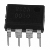
FSQ100
Manufacturer Part Number
FSQ100
Description
IC SWIT PWM GREEN OVP HV 8DIP
Manufacturer
Fairchild Semiconductor
Datasheet
1.FSQ100.pdf
(12 pages)
Specifications of FSQ100
Output Isolation
Isolated
Frequency Range
61 ~ 73kHz
Voltage - Input
8 ~ 20 V
Voltage - Output
650V
Power (watts)
8W
Operating Temperature
25°C ~ 145°C
Package / Case
8-DIP (0.300", 7.62mm)
Power Switch Family
FSQ100
Power Switch On Resistance
16Ohm
Output Current
475mA
Number Of Outputs
Single
Mounting
Through Hole
Supply Current
1.5mA
Package Type
PDIP W
Operating Temperature (min)
-25C
Operating Temperature (max)
85C
Operating Temperature Classification
Commercial
Pin Count
8
Power Dissipation
1.4W
On Resistance (max)
16 Ohms
Maximum Operating Temperature
+ 85 C
Minimum Operating Temperature
- 25 C
Maximum Power Dissipation
1400 mW
Mounting Style
Through Hole
Lead Free Status / RoHS Status
Lead free / RoHS Compliant
Available stocks
Company
Part Number
Manufacturer
Quantity
Price

Part Number:
FSQ100
Manufacturer:
FAIRCHILD/仙童
Quantity:
20 000


© 2007 Fairchild Semiconductor Corporation
FSQ100 Rev. 1.0.2
Pin Assignments
Pin Definitions
Pin #
6,7,8
1
2
3
4
5
Name
Drain
GND
V
V
V
NC
STR
CC
FB
Ground. SenseFET source terminal on primary-side and internal control ground.
Positive Supply Voltage Input. Although connected to an auxiliary transformer winding,
current is supplied from pin 5 (V
V
is supplied via the auxiliary transformer winding.
Feedback. Inverting input to the PWM comparator with its normal input level lies between 0.5V
and 2.5V. It has a 0.4mA current source connected internally, while a capacitor and opto-
coupler are typically connected externally. A feedback voltage of 4.5V triggers overload
protection (OLP). There is a time delay while charging external capacitor C
using an internal 5µA current source. This time delay prevents false triggering under transient
conditions, but still allows the protection mechanism to operate in true overload conditions.
No Connection.
Startup. This pin connects directly to the rectified AC line voltage source. At startup, the internal
switch supplies internal bias and charges an external storage capacitor placed between the V
pin and ground. Once the V
SenseFET Drain. The drain pins are designed to connect directly to the primary lead of the
transformer and are capable of switching a maximum of 650V. Minimizing the length of the trace
connecting these pins to the transformer decreases leakage inductance.
CC
reaches the UVLO upper threshold (9V), the internal startup switch opens and device power
Figure 3.
GND
V
V
NC
CC
FB
Pin Configuration (Top View)
CC
1
2
3
4
reaches 9V, the internal switch stops charging the capacitor.
STR
) via an internal switch during startup (see Figure 2). When
3
Description
8
7
6
5
Drain
Drain
Drain
V
STR
fb
from 3V to 4.5V
www.fairchildsemi.com
CC
Related parts for FSQ100
Image
Part Number
Description
Manufacturer
Datasheet
Request
R

Part Number:
Description:
Fairchild Semiconductor [IGBT MODULE]
Manufacturer:
Fairchild Semiconductor
Datasheet:

Part Number:
Description:
Discrete Semiconductor Modules
Manufacturer:
Fairchild Semiconductor
Part Number:
Description:
Discrete Semiconductor Modules
Manufacturer:
Fairchild Semiconductor
Part Number:
Description:
This N-Channel MOSFET is produced using Fairchild Semiconductor’s advanced Power Trench® process
Manufacturer:
Fairchild Semiconductor
Datasheet:
Part Number:
Description:
This N-Channel MOSFET is produced using Fairchild Semiconductor’s advanced Power Trench® process
Manufacturer:
Fairchild Semiconductor
Datasheet:
Part Number:
Description:
This N-Channel MOSFET is produced using Fairchild Semiconductor’s advanced PowerTrench® process
Manufacturer:
Fairchild Semiconductor
Datasheet:
Part Number:
Description:
This N-Channel MOSFET is produced using Fairchild Semiconductor’s advanced PowerTrench® process
Manufacturer:
Fairchild Semiconductor
Datasheet:
Part Number:
Description:
This N-Channel MOSFET is produced using Fairchild Semiconductor’s advanced Power Trench® process
Manufacturer:
Fairchild Semiconductor
Datasheet:
Part Number:
Description:
This N-Channel logic Level MOSFETs are produced using Fairchild Semiconductor‘s advanced Power Trench® process that has been special tailored to minimize the on-state resistance and yet maintain superior switching performance
Manufacturer:
Fairchild Semiconductor
Datasheet:
Part Number:
Description:
This N-Channel MOSFET is produced using Fairchild Semiconductor’s advanced Power Trench® process
Manufacturer:
Fairchild Semiconductor
Datasheet:
Part Number:
Description:
This N-Channel SyncFET™ is produced using Fairchild Semiconductor’s advanced PowerTrench® process
Manufacturer:
Fairchild Semiconductor
Datasheet:
Part Number:
Description:
This N-Channel SyncFET™ is produced using Fairchild Semiconductor’s advanced PowerTrench® process
Manufacturer:
Fairchild Semiconductor
Datasheet:
Part Number:
Description:
This N-Channel SyncFET™ is produced using Fairchild Semiconductor’s advanced PowerTrench® process
Manufacturer:
Fairchild Semiconductor
Datasheet:
Part Number:
Description:
This N-Channel logic Level MOSFETs are produced using Fairchild Semiconductor‘s advanced Power Trench® process that has been special tailored to minimize the on-state resistance and yet maintain superior switching performance
Manufacturer:
Fairchild Semiconductor
Datasheet:
Part Number:
Description:
This N-Channel MOSFET is produced using Fairchild Semiconductor’s advanced Power Trench® process that has been especially tailored to minimize the on-state resistance and yet maintain superior switching performance
Manufacturer:
Fairchild Semiconductor
Datasheet: