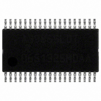
A3985SLDTR-T Allegro Microsystems Inc, A3985SLDTR-T Datasheet - Page 12

A3985SLDTR-T
Manufacturer Part Number
A3985SLDTR-T
Description
IC MOSFET DRVR PROG DUAL 38TSSOP
Manufacturer
Allegro Microsystems Inc
Datasheet
1.A3985SLDTR-T.pdf
(15 pages)
Specifications of A3985SLDTR-T
Configuration
H Bridge
Input Type
Non-Inverting
Delay Time
120ns
Number Of Configurations
2
Number Of Outputs
8
Voltage - Supply
12 V ~ 50 V
Operating Temperature
-20°C ~ 85°C
Mounting Type
Surface Mount
Package / Case
38-TSSOP
Device Type
Full Bridge
Module Configuration
Full Bridge
Peak Output Current
500nA
Output Resistance
19ohm
Input Delay
120ns
Output Delay
120ns
Supply Voltage Range
12V To 50V
Lead Free Status / RoHS Status
Lead free / RoHS Compliant
Current - Peak
-
High Side Voltage - Max (bootstrap)
-
Lead Free Status / RoHS Status
Lead free / RoHS Compliant, Lead free / RoHS Compliant
Other names
620-1180-2
Available stocks
Company
Part Number
Manufacturer
Quantity
Price
Part Number:
A3985SLDTR-T
Manufacturer:
ALLEGRO/雅丽高
Quantity:
20 000
A3985
Note that, for t
full fast-decay mode.
D12 and D13 – Master Clock Control An internal
oscillator can be used for the timing functions, and if more
precise control is required, an external clock can be input to
the OSC terminal (for configuration information, refer to the
Functional Description section). To accommodate a wider
range of external system clocks, an internal divider is pro-
vided to generate the desired master clock frequency, f
according to the following table:
D14 and D15 – Synchronous Rectification Two bits
are used to set the mode for synchronous rectification. The
Bit Assignments Table
Word
*4 MHz typical, configurable with external resistor, ROSC.
0
D13
0
0
1
1
D10
D12
D13
D14
D15
D16
D17
D18
D11
Bit
D0
D1
D2
D3
D4
D5
D6
D7
D8
D9
D12
FD
0
1
0
1
> t
Register Select = 0
Bridge 1, DAC bit 0 (LSB)
Bridge 1, DAC bit 1
Bridge 1, DAC bit 2
Bridge 1, DAC bit 3
Bridge 1, DAC bit 4
Bridge 1, DAC bit 5 (MSB)
Bridge 1, Phase
Bridge 1, Mode
Bridge 2, DAC bit 0 (LSB)
Bridge 2, DAC bit 1
Bridge 2, DAC bit 2
Bridge 2, DAC bit 3
Bridge 2, DAC bit 4
Bridge 2, DAC bit 5 (MSB)
Bridge 2, Phase
Bridge 2, Mode
Range Select bit 0
Range Select bit 1
OFF
Data Register
Master Clock Source and f
, the device effectively operates in
Internal oscillator*
External clock rate
External clock rate / 2
External clock rate / 4
Function
MCK
MCK
,
Dual Full-Bridge MOSFET Driver
Word
1
modes are described in the synchronous rectification section
of the Functional Description section.
D16 and D17 – Reserved These bits are reserved for
testing and should be programmed to 0 during normal
operation.
D18 – Idle Mode The device can be placed in a low
power mode by writing a 0 to D18. This disables the VREG
regulator (to 0 V) and the outputs, and the device draws a
lower load supply current. The undervoltage monitor circuit
remains active. When leaving idle mode, D18 should be set
to 1 for at least 1 ms to allow the regulator to return VREG
to its normal operating voltage (≈12 V) before attempting to
enable any output driver.
D10
D12
D13
D14
D15
D16
D17
D18
D11
Bit
D0
D1
D2
D3
D4
D5
D6
D7
D8
D9
D15
0
0
1
1
Register Select = 1
Blank-time bit 0 (LSB)
Blank-time bit 1 (MSB)
Off-time bit 0 (LSB)
Off-time bit 1
Off-time bit 2
Off-time bit 3
Off-time bit 4 (MSB)
Fast-decay time bit 0 (LSB)
Fast-decay time bit 1
Fast-decay time bit 2
Fast-decay time bit 3 (MSB)
Master Clock Control bit 0 (LSB)
Master Clock Control bit 1 (MSB)
Synchronous Rectification Control bit 0 (LSB)
Synchronous Rectification Control bit 1 (MSB)
Reserved
Reserved
Idle Mode
Digitally Programmable
D14
Control Register
0
1
0
1
115 Northeast Cutoff
1.508.853.5000; www.allegromicro.com
Allegro MicroSystems, Inc.
Worcester, Massachusetts 01615-0036 U.S.A.
Rectification Mode
Synchronous
Function
Disabled
Disabled
Passive
Active
12


