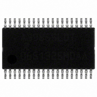
A3985SLDTR-T Allegro Microsystems Inc, A3985SLDTR-T Datasheet - Page 7

A3985SLDTR-T
Manufacturer Part Number
A3985SLDTR-T
Description
IC MOSFET DRVR PROG DUAL 38TSSOP
Manufacturer
Allegro Microsystems Inc
Datasheet
1.A3985SLDTR-T.pdf
(15 pages)
Specifications of A3985SLDTR-T
Configuration
H Bridge
Input Type
Non-Inverting
Delay Time
120ns
Number Of Configurations
2
Number Of Outputs
8
Voltage - Supply
12 V ~ 50 V
Operating Temperature
-20°C ~ 85°C
Mounting Type
Surface Mount
Package / Case
38-TSSOP
Device Type
Full Bridge
Module Configuration
Full Bridge
Peak Output Current
500nA
Output Resistance
19ohm
Input Delay
120ns
Output Delay
120ns
Supply Voltage Range
12V To 50V
Lead Free Status / RoHS Status
Lead free / RoHS Compliant
Current - Peak
-
High Side Voltage - Max (bootstrap)
-
Lead Free Status / RoHS Status
Lead free / RoHS Compliant, Lead free / RoHS Compliant
Other names
620-1180-2
Available stocks
Company
Part Number
Manufacturer
Quantity
Price
Part Number:
A3985SLDTR-T
Manufacturer:
ALLEGRO/雅丽高
Quantity:
20 000
A3985
Basic Operation
The A3985 is a highly-configurable dual full-bridge FET
driver with built-in digital current control. All features are
accessed through a simple SPI (Serial Peripheral Interface)
compatible serial port, allowing multiple motors to be con-
trolled with as few as three wires.
Because the full-bridge control circuits are independently
controlled, the A3985 can be used to drive 2-phase bipolar
stepper motors and 2-phase brushless dc (BLDC) motors.
The current in each of the two external power full-bridges
(which are all N-channel MOSFETs) is regulated by a fixed
off-time PWM control circuit. The full-bridge current at each
step is set by the value of an external current sense resistor,
R
voltage, V
serial data.
The use of PWM with N-channel MOSFETs provides the
most cost-effective solution for a high efficiency motor drive.
The A3985 provides all the necessary circuits to ensure
that the gate-source voltage of both high-side and low-side
external MOSFETs are above 10 V, and that there is no cross-
conduction (shoot through) in the external bridge. Specific
functions are described more fully in the following sections.
Power Supplies
Two power connections are required. The motor power sup-
ply should be connected to VBB to provide the gate drive
levels. Power for internal logic is provided by the VDD
input. Internal logic is designed to operate from 3 to 5.5 V,
allowing the use of 3.3 or 5 V external logic interface cir-
cuits.
GND The ground pin is a reference voltage for internal logic
and analog circuits. There is no large current flow through
this pin. To avoid any noise from switching circuits, this
should have an independent trace to the supply ground star
point.
VREG The voltage at this pin is generated by a low-drop-out
linear regulator from the VBB supply. It is used to oper-
ate the low-side gate drive outputs, GLxx, and to provide
the charging current for the bootstrap capacitors, CBOOTx.
SENSEX
, in the ground connection to the bridge, a reference
REF
, and the output of the DAC controlled by the
Functional Description
Dual Full-Bridge MOSFET Driver
To limit the voltage drop when the charge current is pro-
vided, this pin should be decoupled with a ceramic capaci-
tor, CREG, to ground. The value C
be 40 times the value of the bootstrap capacitor for PWM
frequencies up to 14 kHz. Above 14 kHz, the minimum
recommended value can be determined from the following
formula:
where C
PWM frequency, in kHz. V
age becomes too low, the outputs will be disabled.
REF The reference voltage, V
maximum (100%) peak current. The REF input is internally
limited to 2 V when a 20 kpull-up resistor is connected
between VREF and VDD. This allows the maximum refer-
ence voltage to be set without the need for an externally-
generated voltage. An external reference voltage below the
maximum can also be input on this pin. The voltage at VREF
is divided by the range select ratio G
reference voltage level.
OSC The PWM timing is based on a master clock, typically
running at 4 MHz. The master clock period is used to derive
the PWM off-time, dead time, and blanking time.
The master clock frequency can be set by an internal oscil-
lator or by one of three division ratios of an external clock.
These four options are selected by bits D12 and D13 of the
Control register word.
When the A3985 is configured to use an external clock,
this is input on the OSC pin and will usually provide more
precision than using the internal oscillator. The three internal
divider alternatives provide flexibility in setting the master
clock frequency based on available external system clocks.
If internal timing is selected, f
an external resistor, ROSC, connected from the OSC pin to
GND. This sets the frequency (in MHz) to approximately:
where R
OSC
REG
, in k, is typically between 50 k and 10 k.
and C
C
f
OSC
REG
Digitally Programmable
≈ 100 / (6 + 1.9 × R
BOOT
> C
BOOT
are in nF, and f
REG
115 Northeast Cutoff
1.508.853.5000; www.allegromicro.com
Allegro MicroSystems, Inc.
Worcester, Massachusetts 01615-0036 U.S.A.
× 3 × f
OSC
REF
is monitored, and if the volt-
, at this pin sets the
is configured by using
REG
PWM
m
OSC
to produce the DAC
should typically
PWM
,
) ,
is the maximum
7


