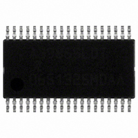
A3985SLDTR-T Allegro Microsystems Inc, A3985SLDTR-T Datasheet - Page 13

A3985SLDTR-T
Manufacturer Part Number
A3985SLDTR-T
Description
IC MOSFET DRVR PROG DUAL 38TSSOP
Manufacturer
Allegro Microsystems Inc
Datasheet
1.A3985SLDTR-T.pdf
(15 pages)
Specifications of A3985SLDTR-T
Configuration
H Bridge
Input Type
Non-Inverting
Delay Time
120ns
Number Of Configurations
2
Number Of Outputs
8
Voltage - Supply
12 V ~ 50 V
Operating Temperature
-20°C ~ 85°C
Mounting Type
Surface Mount
Package / Case
38-TSSOP
Device Type
Full Bridge
Module Configuration
Full Bridge
Peak Output Current
500nA
Output Resistance
19ohm
Input Delay
120ns
Output Delay
120ns
Supply Voltage Range
12V To 50V
Lead Free Status / RoHS Status
Lead free / RoHS Compliant
Current - Peak
-
High Side Voltage - Max (bootstrap)
-
Lead Free Status / RoHS Status
Lead free / RoHS Compliant, Lead free / RoHS Compliant
Other names
620-1180-2
Available stocks
Company
Part Number
Manufacturer
Quantity
Price
Part Number:
A3985SLDTR-T
Manufacturer:
ALLEGRO/雅丽高
Quantity:
20 000
A3985
Current Sensing
To minimize inaccuracies in sensing the I
level caused by ground-trace IR drops, the sense resistor,
RSENSEx, should have an independent return to the supply
ground star point. For low-value sense resistors, the IR drops
in the sense resistor PCB traces can be significant and should
be taken into account. The use of sockets should be avoided
as they can introduce variation in RENSE
contact resistance.
Thermal Protection
All drivers are turned off when the junction temperature
reaches 165°C typical. This is intended only to protect the
A3985 from failures due to excessive junction temperatures.
Thermal protection will not protect the A3985 from continu-
ous short circuits. Thermal shutdown has a hysteresis of
approximately 15°C.
Circuit Layout
Since this is a switch-mode application, where rapid current
changes are present, care must be taken during layout of the
application PCB. The following points are provided as guid-
ance for layout. Following all guidelines will not always be
possible. However, each point should be carefully considered
as part of any layout procedure.
Ground Connection Layout Recommendations:
1. Decoupling capacitors for the supply pins VBB, VREG,
and VDD should be connected independently, close to the
GND pin, and not to any ground plane. The decoupling
capacitors should also be connected as close as possible to
the corresponding supply pin.
2. If used, the oscillator timing resistor ROSC should be
connected to the GND pin. It should not be connected to any
ground plane, supply common, or the power ground.
PEAK
Sx
Applications Information
due to their
current
Dual Full-Bridge MOSFET Driver
3. The GND pin should be connected by an independent low-
impedance trace to the supply common at a single point.
4. Check the peak voltage excursion of the transients on
the LSS pin with reference to the GND pin using a close
grounded (tip and barrel) probe. If the voltage at LSS
exceeds the specified absolute maximum add additional
clamping, capacitance, or both, between the LSS pin and the
AGND pin.
Other layout recommendations:
1. Gate charge drive paths and gate discharge return paths
may carry transient current pulses. Therefore, the traces from
GHxx, GLxx, Sxx, and LSSx should be as short as possible to
reduce the inductance of the circuit trace.
2. Provide an independent connection from each LSS pin
to the common point of each power bridge. It is not recom-
mended to connect LSS directly to the GND pin. The LSS
connection should not be used for the SENSE connection.
3. Minimize stray inductance by using short, wide copper
runs at the drain and source terminals of all power FETs.
This includes motor lead connections, the input power bus,
and the common source of the low-side power FETs. This
will minimize voltages induced by fast switching of large
load currents.
4. Consider the use of small (100nF) ceramic decoupling
capacitors across the source and drain of the power FETs to
limit fast transient voltage spikes caused by trace inductance.
The above are only recommendations. Each application is
different and may encounter different sensitivities. Each
design should be tested at the maximum current, to ensure
any parasitic effects are eliminated.
Digitally Programmable
115 Northeast Cutoff
1.508.853.5000; www.allegromicro.com
Allegro MicroSystems, Inc.
Worcester, Massachusetts 01615-0036 U.S.A.
13


