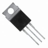
BTS117 Infineon Technologies, BTS117 Datasheet - Page 4

BTS117
Manufacturer Part Number
BTS117
Description
IC LOW SIDE SW PWR 3.5A TO-220-3
Manufacturer
Infineon Technologies
Series
HITFET®r
Type
Low Sider
Specifications of BTS117
Input Type
Non-Inverting
Number Of Outputs
1
On-state Resistance
80 mOhm
Current - Output / Channel
3.5A
Current - Peak Output
25A
Voltage - Supply
2.2 V ~ 10 V
Operating Temperature
-40°C ~ 150°C
Mounting Type
Through Hole
Package / Case
TO-220-2
Module Configuration
Low Side
Peak Output Current
3.5A
Output Resistance
0.08ohm
Input Delay
40µs
Output Delay
70µs
Supply Voltage Range
1.3V To 10V
Driver Case Style
TO-220
No. Of Pins
3
Packages
P-TO220-3
Channels
1.0
Vds (max)
60.0 V
Id(nom)
3.5 A
Rds (on) (max)
100.0 mOhm
Id(lim) (min)
7.0 A
Lead Free Status / RoHS Status
Contains lead / RoHS non-compliant
Other names
BTS117IN
BTS117NK
SP000011195
BTS117NK
SP000011195
Available stocks
Company
Part Number
Manufacturer
Quantity
Price
Part Number:
BTS117
Manufacturer:
INFINEON/英飞凌
Quantity:
20 000
Company:
Part Number:
BTS117 E3045A
Manufacturer:
INFINEON
Quantity:
354
Company:
Part Number:
BTS117E3045A
Manufacturer:
NSC
Quantity:
15 562
Company:
Part Number:
BTS117TC
Manufacturer:
INFIINION
Quantity:
471
Part Number:
BTS117TC
Manufacturer:
INFINEON/英飞凌
Quantity:
20 000
Datasheet
2 Integrated protection functions are designed to prevent IC destruction under fault conditions
described in the data sheet. Fault conditions are considered as "outside" normal operating range.
Protection functions are not designed for continuous repetitive operation.
1 Device switched on into existing short circuit (see diagram Determination of I D(lim) ). If the device is in on condition
and a short circuit occurs, these values might be exceeded for max. 50 µs.
Characteristics
Initial peak short circuit current limit
V
Current limit
V
T
Dynamic Characteristics
Turn-on time
R
Turn-off time
R
Slew rate on
R
Slew rate off
R
Protection Functions
Thermal overload trip temperature
Unclamped single pulse inductive energy
I
I
Inverse Diode
Inverse diode forward voltage
I
Electrical Characteristics
Parameter
at T
D
D
F
j
IN
IN
L
L
L
L
= -40...+150 °C
= 5*3.5A, t
= 3.5 A, T
= 3.5 A, T
= 4.7 Ω, V
= 4.7 Ω, V
= 4.7 Ω, V
= 4.7 Ω, V
= 10 V, V
= 10 V, V
j
=25°C, unless otherwise specified
j
j
1)
m
DS
DS
IN
IN
IN
IN
= 25 °C, V
= 150 °C, V
= 300 µS, V
= 0 to 10 V, V
= 10 to 0 V, V
= 0 to 10 V, V
= 10 to 0 V, V
= 12 V
= 12 V, t
V
V
70 to 50% V
50 to 70% V
IN
IN
to 90% I
to 10% I
bb
m
bb
2)
= 32 V
IN
= 350 µs,
= 32 V
D
D
bb
bb
bb
bb
= 0 V
bb
bb
:
:
= 12 V
= 12 V
= 12 V
= 12 V
:
:
4
I
I
t
t
-dV
dV
T
E
V
Symbol
D(SCp)
D(lim)
on
off
jt
AS
SD
DS
DS
/dt
/dt
off
on
Smart Low Side Power Switch
1000
min.
225
150
7
-
-
-
-
-
-
Values
typ.
165
25
10
40
70
--
--
1
1
1
Rev. 1.3, 2008-12-10
HITFET BTS 117
max.
150
15
70
--
--
3
3
-
-
-
A
µs
V/µs
°C
mJ
V
Unit


