AMIS30622C6228G ON Semiconductor, AMIS30622C6228G Datasheet - Page 25

AMIS30622C6228G
Manufacturer Part Number
AMIS30622C6228G
Description
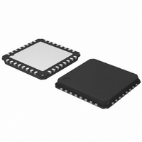
IC MOTOR DVR MICROSTP I2C 32NQFP
Manufacturer
ON Semiconductor
Type
Micro Stepping Motor Driverr
Datasheet
1.AMIS30622C6227RG.pdf
(50 pages)
Specifications of AMIS30622C6228G
Applications
Stepper Motor Driver
Number Of Outputs
1
Current - Output
800mA
Voltage - Supply
6.5 V ~ 29 V
Operating Temperature
-40°C ~ 125°C
Mounting Type
Surface Mount
Package / Case
32-VSQFP
Operating Supply Voltage
5 V
Mounting Style
SMD/SMT
Lead Free Status / RoHS Status
Lead free / RoHS Compliant
Voltage - Load
-
Lead Free Status / Rohs Status
Lead free / RoHS Compliant
Available stocks
Company
Part Number
Manufacturer
Quantity
Price
Company:
Part Number:
AMIS30622C6228G
Manufacturer:
ON Semiconductor
Quantity:
71
Company:
Part Number:
AMIS30622C6228G
Manufacturer:
ON Semiconductor
Quantity:
10 000
<UV2> flag is set. In case V
updates of the target position by means of the reception of
SetPosition or GotoSecurePosition commands,
only AFTER the <UV2> flag is cleared by receiving a
GetFullStatus1 or GetFullStatus2 command.
in shutdown state. The <UV2> and <Steploss> flags are
set. In case V
target position by means of the reception of SetPosition
or GotoSecurePosition commands, only AFTER the
<UV2> and <Steploss> flags are cleared by receiving a
GetFullStatus1 or GetFullStatus2 command.
OTP Register
OTP Memory Structure
<LOCKBT> are already programmed in the OTP memory at
circuit delivery. They correspond to the calibration of the
circuit and are just documented here as an indication.
set it to ‘1’. Thus only bits having to be at ‘1’ must be zapped.
Zapping of a bit already at ‘1’ is disabled. Each OTP byte
will
SetOTPparam). Once OTP programming is completed, bit
<LOCKBG> can be zapped to disable future zapping,
otherwise any OTP bit at ‘0’ could still be zapped by using
a SetOTPparam command.
the I
Table 17. OTP MEMORY STRUCTURE
Table 18. OTP OVERWRITE PROTECTION
LOCKBT
before delivery)
LOCKBG
Address
In Stop mode 1 the motor is put in shutdown state. The
In Stop mode 2 the motor is stopped immediately and put
The table below shows how the parameters to be stored in the OTP memory are located.
Parameters stored at address 0x00 and 0x01 and bit
Each OTP bit is at ‘0’ when not zapped. Zapping a bit will
The command used to load the application parameters via
0x00
0x01
0x02
0x03
0x04
0x05
0x06
0x07
2
C bus in the RAM prior to an OTP Memory
be
Lock Bit
(factory zapped
BB
programmed
SecPos10
SecPos7
Vmax3
> UV1, AMIS−30622 accepts updates of the
OSC3
Irun3
Bit 7
0
BB
SecPos9
SecPos6
separately
Vmax2
> UV1, AMIS−30622 accepts
OSC2
TSD2
Bit 6
Irun2
Protected Bytes
0x00 to 0x01
0x00 to 0x07
(see
SecPos8
SecPos5
Vmax1
OSC1
TSD1
Irun1
Bit 5
command
http://onsemi.com
SecPos4
Vmax0
OSC0
TSD0
Irun0
Shaft
Bit 4
25
Important Notes:
•
•
•
programming is SetMotorParam. This allows for a
functional verification before using a SetOTPparam
command to program and zap separately one OTP memory
byte. A GetOTPparam command issued after each
SetOTPparam command allows verifying the correct byte
zapping.
Note: Zapped bits will become active only after a power
cycle. After programming the I
to be performed first to guarantee further communication
with the device.
Application Parameters Stored in OTP Memory
parameters, although programmed in a non−volatile
memory can still be overridden in RAM by a I
operation.
Except for the physical address <PA[3:0]> these
In the case of Stop mode 2, care needs to be taken
because the accumulated steploss can cause a
significant deviation between physical and stored actual
position.
The SetDualPosition command will only be
executed after clearing the <UV2> and <Steploss>
flags.
RAM reset occurs when V
level).
PA[3:0] In combination with hired wired (HW)
StepMode1
SecPos3
IREF3
Vmin3
Ihold3
Acc3
Bit 3
BG3
PA3
address, it forms the physical address AD[6:0]
of the stepper−motor. Up to 32 stepper motors
can theoretically be connected to the same I
bus.
StepMode0
SecPos2
IREF2
Vmin2
Ihold2
Acc2
Bit 2
BG2
PA2
DD
2
C bits the power cycle has
< V
SecPos1
LOCKBT
IREF1
Vmin1
Ihold1
Bit 1
Acc1
BG1
PA1
DD
Reset (digital POR
LOCKBG
SecPos0
2
IREF0
Ihold0
Vmin0
C writing
Bit 0
Acc0
BG0
PA0
2
C


