AMIS30622C6228G ON Semiconductor, AMIS30622C6228G Datasheet - Page 39
AMIS30622C6228G
Manufacturer Part Number
AMIS30622C6228G
Description
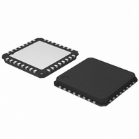
IC MOTOR DVR MICROSTP I2C 32NQFP
Manufacturer
ON Semiconductor
Type
Micro Stepping Motor Driverr
Datasheet
1.AMIS30622C6227RG.pdf
(50 pages)
Specifications of AMIS30622C6228G
Applications
Stepper Motor Driver
Number Of Outputs
1
Current - Output
800mA
Voltage - Supply
6.5 V ~ 29 V
Operating Temperature
-40°C ~ 125°C
Mounting Type
Surface Mount
Package / Case
32-VSQFP
Operating Supply Voltage
5 V
Mounting Style
SMD/SMT
Lead Free Status / RoHS Status
Lead free / RoHS Compliant
Voltage - Load
-
Lead Free Status / Rohs Status
Lead free / RoHS Compliant
Available stocks
Company
Part Number
Manufacturer
Quantity
Price
Company:

Part Number:
AMIS30622C6228G
Manufacturer:
ON Semiconductor
Quantity:
71
Company:
Part Number:
AMIS30622C6228G
Manufacturer:
ON Semiconductor
Quantity:
10 000


Notes:
7−bit Addressing
first byte after the START condition usually determines
which slave will be selected by the master. The exception is
the general call address which can call all devices. When this
address is used all devices should respond with an
acknowledge. The second byte of the general call address
then defines the action to be taken.
Definition of Bits in the First Byte
address. The eighth bit is the least significant bit (LSB). It
determines the direction of the message. If the LSB is a
“zero” it means that the master will write information to a
selected slave. A “one” in this position means that the master
will read information from the slave. When an address is
sent, each device in a system compares the first seven bits
after the START condition with its address. If they match,
the device considers itself addressed by the master as a
slave−receiver or slave−transmitter, depending on the R/W
bit.
The addressing procedure for the I
The first seven bits of the first byte make up the slave
2. The second transmission consists of the slave
1. Each byte is followed by an acknowledgment bit as indicated by the A or A in the sequence.
2. I
3. A START condition immediately followed by a STOP condition (void message) is an illegal format.
Figure 31. First Byte after START Procedure
address and the read bit. Then the master can read
the data bits on the SDA line on every rising edge
of signal SCK. After each byte of data the master
has to acknowledge correct data reception by
slave address, even if these START conditions are not positioned according to the proper format.
2
MSB
C−bus compatible devices must reset their bus logic on receipt of a START condition such that they all anticipate the sending of a
Figure 30. Master Reading Data from AMIS−30622: Second Transmission is Reading Data
Figure 29. Master Reading Data from AMIS−30622: First Transmission is Addressing
SLAVE ADDRESS
S
Master to AMIS− 30624
AMIS− 30624 to Master
Slave Address
S
2
C−bus is such that the
Slave Address
”0” = WRITE
R/W
R/W
LSB
A
http://onsemi.com
”0” = WRITE
S = Start condition
P = Stop condition
A = Acknowledge (SDA = LOW)
A = No Acknowledge (SDA = HIGH)
R/W
Data
39
A
to discriminate this circuit from other circuits on the I
This address is coded on seven bits (two bits being internally
hardwired to ‘1’), yielding the theoretical possibility of 32
different circuits on the same bus. It is a combination of four
OTP memory bits (OTP Memory Structure OPEN) and of
the externally hardwired address bits (pin HW). HW must
either be connected to ground or to V
connected and is left floating, correct functionality of the
positioner is not guaranteed. The motor will be driven to the
programmed secure position (See Hardwired Address –
OPEN).
General Call Address
“000 0000”, which can address all devices. When this
address is used all devices should respond with an
acknowledge. The second byte of the general call address
then defines the action to be taken.
N bytes + Acknowledge
Internal Address
AMIS−30622 is provided with a physical address in order
The AMIS−30622 supports also a “general call” address
MSB
1
Figure 32. First Byte after START Procedure
pulling SDA LOW. The last byte is not
acknowledged by the master and therefore the
slave knows the end of transmission.
A
1
PA3 PA2 PA1 PA0 HW
OTP memory
Data
A
P
A
Hardwired Address Bit
bat
P
R/W
. When HW is not
LSB
2
C bus.
Related parts for AMIS30622C6228G
Image
Part Number
Description
Manufacturer
Datasheet
Request
R

Part Number:
Description:
ON Semiconductor [VOLTAGE REGULATOR]
Manufacturer:
ON Semiconductor
Datasheet:
Part Number:
Description:
357-036-542-201 CARDEDGE 36POS DL .156 BLK LOPRO
Manufacturer:
ON Semiconductor
Datasheet:
Part Number:
Description:
357-036-542-201 CARDEDGE 36POS DL .156 BLK LOPRO
Manufacturer:
ON Semiconductor
Datasheet:
Part Number:
Description:
357-036-542-201 CARDEDGE 36POS DL .156 BLK LOPRO
Manufacturer:
ON Semiconductor
Datasheet:
Part Number:
Description:
357-036-542-201 CARDEDGE 36POS DL .156 BLK LOPRO
Manufacturer:
ON Semiconductor
Datasheet:
Part Number:
Description:
357-036-542-201 CARDEDGE 36POS DL .156 BLK LOPRO
Manufacturer:
ON Semiconductor
Datasheet:
Part Number:
Description:
357-036-542-201 CARDEDGE 36POS DL .156 BLK LOPRO
Manufacturer:
ON Semiconductor
Datasheet:
Part Number:
Description:
357-036-542-201 CARDEDGE 36POS DL .156 BLK LOPRO
Manufacturer:
ON Semiconductor
Datasheet:
Part Number:
Description:
357-036-542-201 CARDEDGE 36POS DL .156 BLK LOPRO
Manufacturer:
ON Semiconductor
Datasheet:
Part Number:
Description:
357-036-542-201 CARDEDGE 36POS DL .156 BLK LOPRO
Manufacturer:
ON Semiconductor
Datasheet:
Part Number:
Description:
357-036-542-201 CARDEDGE 36POS DL .156 BLK LOPRO
Manufacturer:
ON Semiconductor
Datasheet:
Part Number:
Description:
Manufacturer:
ON Semiconductor
Datasheet:
Part Number:
Description:
Manufacturer:
ON Semiconductor
Datasheet:
Part Number:
Description:
Manufacturer:
ON Semiconductor
Datasheet: