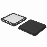
AMIS30622C6228G ON Semiconductor, AMIS30622C6228G Datasheet - Page 38

AMIS30622C6228G
Manufacturer Part Number
AMIS30622C6228G
Description
IC MOTOR DVR MICROSTP I2C 32NQFP
Manufacturer
ON Semiconductor
Type
Micro Stepping Motor Driverr
Datasheet
1.AMIS30622C6227RG.pdf
(50 pages)
Specifications of AMIS30622C6228G
Applications
Stepper Motor Driver
Number Of Outputs
1
Current - Output
800mA
Voltage - Supply
6.5 V ~ 29 V
Operating Temperature
-40°C ~ 125°C
Mounting Type
Surface Mount
Package / Case
32-VSQFP
Operating Supply Voltage
5 V
Mounting Style
SMD/SMT
Lead Free Status / RoHS Status
Lead free / RoHS Compliant
Voltage - Load
-
Lead Free Status / Rohs Status
Lead free / RoHS Compliant
Available stocks
Company
Part Number
Manufacturer
Quantity
Price
Company:
Part Number:
AMIS30622C6228G
Manufacturer:
ON Semiconductor
Quantity:
71
Company:
Part Number:
AMIS30622C6228G
Manufacturer:
ON Semiconductor
Quantity:
10 000
Clock Generation
messages on the I
HIGH period of the clock.
Data Formats with 7−bit Addresses
the START condition (S), a slave address is sent. This
SCK
bus, it can generate a repeated START (Sr) and address
another slave without first generating a STOP condition.
Various combinations of read/write formats are then
possible within such a transfer.
Data Transfer Formats
Writing Data to AMIS−30622
transmits to slave−receiver and the transfer direction is not
changed. A complete transmission consists of:
eight bytes of data, other commands are transmitting two
bytes of data. See Table 25.
Reading Data to AMIS−30622
are needed:
SDA
The master generates the clock on the SCK line to transfer
Data transfers follow the format shown in Figure 27. After
However, if a master still wishes to communicate on the
When writing to AMIS−30622, the master−transmitter
Some commands for the AMIS−30622 are supporting
When reading data from AMIS−30622 two transmissions
♦
♦
Start condition
The slave address (7−bit)
condition
START
START
S
ADDRESS
2
C−bus. Data is only valid during the
1 − 7
Master to AMIS− 30624
AMIS− 30624 to Master
Slave Address
R/W
8
Figure 28. Master Writing Data to AMIS−30622
”0” = WRITE
ACK
9
R/W
Figure 27. A Complete Data Transfer
A
http://onsemi.com
S = Start condition
P = Stop condition
A = Acknowledge (SDA = LOW)
A = No Acknowledge (SDA = HIGH)
1 − 7
DATA
Data
38
address is 7−bit long followed by an eighth bit which is a data
direction bit (R/W) − a ‘zero’ indicates a transmission
(WRITE), a ‘one’ indicates a request for data (READ). A
data transfer is always terminated by a STOP condition (P)
generated by the master.
N bytes + Acknowledge
8
♦
♦
♦
♦
1. The first transmission consists of two bytes of
acknowledge bit. The acknowledge bit is used to
signal a correct reception of the data to the
transmitter. In this case the AMIS−30622 pulls the
SDA line to ‘0’. The AMIS−30622 reads the
incoming data at SDA on every rising edge of the
SCK signal
Read/Write bit (‘0’ = write)
Acknowledge bit
Any further data bytes are followed by an
Stop condition to finish the transmission
data:
♦
♦
A
ACK
9
The first byte contains the slave address and the
The second byte contains the address of an
write bit.
internal register in the
AMIS−30622. This internal
register address is stored in the circuit RAM.
Data
1 − 7
DATA
A
8
P
ACK
9
condition
STOP
STOP


