AMIS30622C6228G ON Semiconductor, AMIS30622C6228G Datasheet - Page 36
AMIS30622C6228G
Manufacturer Part Number
AMIS30622C6228G
Description
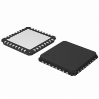
IC MOTOR DVR MICROSTP I2C 32NQFP
Manufacturer
ON Semiconductor
Type
Micro Stepping Motor Driverr
Datasheet
1.AMIS30622C6227RG.pdf
(50 pages)
Specifications of AMIS30622C6228G
Applications
Stepper Motor Driver
Number Of Outputs
1
Current - Output
800mA
Voltage - Supply
6.5 V ~ 29 V
Operating Temperature
-40°C ~ 125°C
Mounting Type
Surface Mount
Package / Case
32-VSQFP
Operating Supply Voltage
5 V
Mounting Style
SMD/SMT
Lead Free Status / RoHS Status
Lead free / RoHS Compliant
Voltage - Load
-
Lead Free Status / Rohs Status
Lead free / RoHS Compliant
Available stocks
Company
Part Number
Manufacturer
Quantity
Price
Company:

Part Number:
AMIS30622C6228G
Manufacturer:
ON Semiconductor
Quantity:
71
Company:
Part Number:
AMIS30622C6228G
Manufacturer:
ON Semiconductor
Quantity:
10 000


General Characteristics
a positive supply voltage via a pull−up resistor (see
Figure 22). When the bus is free both lines are HIGH. The
output stages of the devices connected to the bus must have
an open drain to perform the wired−AND function. Data on
the I
The number of interfaces connected to the bus is dependent
on the maximum bus capacitance limit (See C
and the available number of addresses.
Bit Transfer
fixed in the I
level. Using AMIS−30622, the levels are specified in
Table 5. One clock pulse is generated for each data bit
transferred.
Data Validity
period of the clock. The HIGH or LOW state of the data line
can only change when the clock signal on the SCL line is
LOW (See Figure 23).
SCK
Both SDA and SCK are bi−directional lines connected to
The levels for logic ‘0’ (LOW) and ‘1’ (HIGH) are not
The data on the SDA line must be stable during the HIGH
SDA
2
C−bus can be transferred up to 400 kb/s in fast mode.
Serial Data Line
Serial Clock Line
Clock IN
Figure 23. Bit Transfer on the I
AMIS−30624,
Clock OUT
NCV70624
2
C standard but dependent on the used V
Data line stable
−> Data valid
SCK
2
Data IN
Data OUT
data allowed
Change of
Figure 22. Connection of a Device to the I
2
SDA
C−bus
B
in Table 6)
1
http://onsemi.com
DD
Clock IN
36
Clock OUT
MASTER
START and STOP Conditions
arise, which are defined as START (S) and STOP (P)
conditions (See Figure 24).
is HIGH is one such unique case. This situation indicates a
START condition. LOW to HIGH transition on the SDA line
while SCK is HIGH defines a STOP condition.
master. The bus is considered to be busy after the START
condition. The bus is considered to be free again a certain
time after the STOP condition. The bus free situation is
specified as t
instead of a STOP condition. In this respect, the START (S)
and repeated START (Sr) conditions are functionally
identical (See Figure 25). The symbol S will be used to
represent START and repeated START, unless otherwise
noted.
Within the procedure of the I
A HIGH to LOW transition on the SDA line while SCK
START and STOP conditions are always generated by the
The bus stays busy if a repeated START (Sr) is generated
SCK
SDA
SCL
Figure 24. START and STOP Conditions
condition
BUF
START
START
Data IN
2
C−bus
Data OUT
in Table 6.
SDA
2
C−bus, unique situations
+5 V
R
p
condition
STOP
STOP
R
p
Related parts for AMIS30622C6228G
Image
Part Number
Description
Manufacturer
Datasheet
Request
R

Part Number:
Description:
ON Semiconductor [VOLTAGE REGULATOR]
Manufacturer:
ON Semiconductor
Datasheet:
Part Number:
Description:
357-036-542-201 CARDEDGE 36POS DL .156 BLK LOPRO
Manufacturer:
ON Semiconductor
Datasheet:
Part Number:
Description:
357-036-542-201 CARDEDGE 36POS DL .156 BLK LOPRO
Manufacturer:
ON Semiconductor
Datasheet:
Part Number:
Description:
357-036-542-201 CARDEDGE 36POS DL .156 BLK LOPRO
Manufacturer:
ON Semiconductor
Datasheet:
Part Number:
Description:
357-036-542-201 CARDEDGE 36POS DL .156 BLK LOPRO
Manufacturer:
ON Semiconductor
Datasheet:
Part Number:
Description:
357-036-542-201 CARDEDGE 36POS DL .156 BLK LOPRO
Manufacturer:
ON Semiconductor
Datasheet:
Part Number:
Description:
357-036-542-201 CARDEDGE 36POS DL .156 BLK LOPRO
Manufacturer:
ON Semiconductor
Datasheet:
Part Number:
Description:
357-036-542-201 CARDEDGE 36POS DL .156 BLK LOPRO
Manufacturer:
ON Semiconductor
Datasheet:
Part Number:
Description:
357-036-542-201 CARDEDGE 36POS DL .156 BLK LOPRO
Manufacturer:
ON Semiconductor
Datasheet:
Part Number:
Description:
357-036-542-201 CARDEDGE 36POS DL .156 BLK LOPRO
Manufacturer:
ON Semiconductor
Datasheet:
Part Number:
Description:
357-036-542-201 CARDEDGE 36POS DL .156 BLK LOPRO
Manufacturer:
ON Semiconductor
Datasheet:
Part Number:
Description:
Manufacturer:
ON Semiconductor
Datasheet:
Part Number:
Description:
Manufacturer:
ON Semiconductor
Datasheet:
Part Number:
Description:
Manufacturer:
ON Semiconductor
Datasheet: