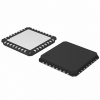
AMIS30622C6228G ON Semiconductor, AMIS30622C6228G Datasheet - Page 37

AMIS30622C6228G
Manufacturer Part Number
AMIS30622C6228G
Description
IC MOTOR DVR MICROSTP I2C 32NQFP
Manufacturer
ON Semiconductor
Type
Micro Stepping Motor Driverr
Datasheet
1.AMIS30622C6227RG.pdf
(50 pages)
Specifications of AMIS30622C6228G
Applications
Stepper Motor Driver
Number Of Outputs
1
Current - Output
800mA
Voltage - Supply
6.5 V ~ 29 V
Operating Temperature
-40°C ~ 125°C
Mounting Type
Surface Mount
Package / Case
32-VSQFP
Operating Supply Voltage
5 V
Mounting Style
SMD/SMT
Lead Free Status / RoHS Status
Lead free / RoHS Compliant
Voltage - Load
-
Lead Free Status / Rohs Status
Lead free / RoHS Compliant
Available stocks
Company
Part Number
Manufacturer
Quantity
Price
Company:
Part Number:
AMIS30622C6228G
Manufacturer:
ON Semiconductor
Quantity:
71
Company:
Part Number:
AMIS30622C6228G
Manufacturer:
ON Semiconductor
Quantity:
10 000
Transferring Data
Byte Format
number of bytes that can be transmitted per transfer to
AMIS−30622 is restricted to eight. Each byte has to be
followed by an acknowledge bit. Data is transferred with the
Acknowledge
acknowledge−related clock pulse is generated by the master.
The transmitter releases the SDA line (HIGH) during the
acknowledge clock pulse. The receiver must pull down the
SDA line during the acknowledge clock pulse so that it
remains stable LOW during the HIGH period of this clock
pulse (see Figure 26). Of course, set−up and hold times must
also taken into account (see Table 6). When AMIS−30622
doesn’t acknowledge the slave address, the data line will be
left HIGH. The master can than generate either a STOP
condition to abort the transfer, or a repeated START
condition to start a new transfer.
SCK
SDA
Every byte put on the SDA line must be 8−bits long. The
Data transfer with acknowledge is obligatory. The
condition
START
START
MSB
1
SDA by master
SDA by slave
transmitter
receiver
SCK from
master
2
condition
START
START
Figure 25. Data Transfer on the I
Figure 26. Acknowledge on the I
7
clock puse from master
MSB
Aknowledge related
Acknowledgement
1
signal from slave
http://onsemi.com
Master releases the Data line
8
2
Not acknowledged
37
9
Acknowledged
clock puse from master
Aknowledge related
most significant bit (MSB) first (See Figure 25). If a slave
can’t receive or transmit another complete byte of data, it can
hold the clock line SCK LOW to force the master into a wait
state. Data transfer then continues when the slave is ready for
another byte of data and releases clock line SCK.
slave address but later in the transfer cannot receive any
more data bytes, this is indicated by generating a
not−acknowledge on the first byte to follow. The master
generates than a STOP or a repeated START condition.
signal the end of data to the slave−transmitter by not
generating an acknowledge on the last byte that was clocked
out of the slave. AMIS−30622 as slave−transmitter shall
release the data line to allow the master to generate STOP or
repeated START condition.
Clock line held
If AMIS−30622 as slave−receiver does acknowledge the
If a master−receiver is involved in the transfer, it must
low by slave
8
2
2
C−bus
C−bus
1
9
2
Slave pulls data line
low if Acknowledged
3−8
ACK
9
condition
STOP
STOP


