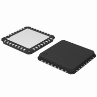
AMIS30622C6228G ON Semiconductor, AMIS30622C6228G Datasheet - Page 8

AMIS30622C6228G
Manufacturer Part Number
AMIS30622C6228G
Description
IC MOTOR DVR MICROSTP I2C 32NQFP
Manufacturer
ON Semiconductor
Type
Micro Stepping Motor Driverr
Datasheet
1.AMIS30622C6227RG.pdf
(50 pages)
Specifications of AMIS30622C6228G
Applications
Stepper Motor Driver
Number Of Outputs
1
Current - Output
800mA
Voltage - Supply
6.5 V ~ 29 V
Operating Temperature
-40°C ~ 125°C
Mounting Type
Surface Mount
Package / Case
32-VSQFP
Operating Supply Voltage
5 V
Mounting Style
SMD/SMT
Lead Free Status / RoHS Status
Lead free / RoHS Compliant
Voltage - Load
-
Lead Free Status / Rohs Status
Lead free / RoHS Compliant
Available stocks
Company
Part Number
Manufacturer
Quantity
Price
Company:
Part Number:
AMIS30622C6228G
Manufacturer:
ON Semiconductor
Quantity:
71
Company:
Part Number:
AMIS30622C6228G
Manufacturer:
ON Semiconductor
Quantity:
10 000
The AC parameters are guaranteed for temperature and V
POWERUP
INTERNAL OSCILLATOR
I
I
Table 6. AC PARAMETERS
15. The maximum number of connected I
16. An I
17. The maximum t
18. A Fast−mode I
2
2
t
t
t
t
C TRANSCEIVER (STANDARD MODE)
t
C TRANSCEIVER (FAST MODE)
t
HD,START
SU,START
t
t
HD,START
SU,START
t
t
Symbol
SU,STOP
SU,STOP
HD,DATA
SU,DATA
HD,DATA
SU,DATA
t
t
t
t
f
t
f
t
to still guarantee the rise and fall times of the bus signals.
the undefined region of the falling edge of SCL.
This will automatically be the case if the device does not stretch the LOW period of the SCL signal. If such a device does stretch the LOW
period of the SCL signal, it must output the next data bit to the SDA line trmax + t
standard−mode I
HIGH
HIGH
LOW
LOW
T
f
SCL
BUF
SCL
BUF
osc
t
t
t
t
pu
R
R
F
F
2
C device must internally provide a hold time of at least 300 ns for the SDA signal (referred to the V
Pin(s)
SDA
SCK
SDA
SCK
2
C−bus device can be used in a standard−mode I
HD,DAT
2
C−bus specification) before the SCL line is released.
Power−up time
Frequency of internal oscillator
SCL clock frequency
Hold time (repeated) START condition. After
this period the first clock pulse is generated.
LOW period of the SCK clock
HIGH period of the SCK clock
Set−up time for a repeated START condition
Data hold time for I
Data set−up time
Rise time of SDA and SCK signals
Fall time of SDA and SCK signals
Set−up time for STOP condition
Bus free time between STOP and START
condition
has only to be met if the device does not stretch the LOW period (t
Parameter
2
C devices is dependent on the number of available addresses and the maximum bus capacitance
2
2
C bus devices
C bus devices
AC PARAMETERS
http://onsemi.com
BB
2
C bus system, but the requirement t
in the operating range unless otherwise specified.
8
Guaranteed by design
Test Conditions
V
BB
= 14 V
SU,DATA
LOW
= 1000 + 250 = 1250 ns (according to the
) of the SCL signal.
(Note 16)
(Note 16)
(Note 18)
0.1 C
0.1 C
20 +
20 +
Min
250
100
3.6
4.0
4.7
4.0
4.7
4.0
4.7
0.6
1.3
0.6
0.6
0.6
1.3
0
0
SU,DATA
B
B
IHmin
w 250 ns must than be met.
Typ
of the SCL signal) to bridge
4.0
(Note 17)
(Note 17)
Max
3.45
100
360
300
300
4.4
1.0
0.3
0.9
10
MHz
Unit
kHz
kHz
ms
ms
ms
ms
ms
ms
ns
ms
ms
ms
ms
ms
ms
ms
ms
ms
ns
ns
ns
ms
ms


