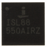
ISL88550AIRZ Intersil, ISL88550AIRZ Datasheet - Page 17

ISL88550AIRZ
Manufacturer Part Number
ISL88550AIRZ
Description
IC PWM CONTROLLER 28TQFN
Manufacturer
Intersil
Datasheet
1.ISL88550AIRZ.pdf
(25 pages)
Specifications of ISL88550AIRZ
Applications
PWM Controller
Voltage - Input
2 ~ 25 V
Current - Supply
25µA
Operating Temperature
-40°C ~ 85°C
Mounting Type
Surface Mount
Package / Case
28-TQFN
Rohs Compliant
YES
Lead Free Status / RoHS Status
Lead free / RoHS Compliant
Voltage - Supply
-
Available stocks
Company
Part Number
Manufacturer
Quantity
Price
Company:
Part Number:
ISL88550AIRZ
Manufacturer:
Intersil
Quantity:
480
Part Number:
ISL88550AIRZ
Manufacturer:
INTERSIL
Quantity:
20 000
Company:
Part Number:
ISL88550AIRZ-T
Manufacturer:
AMD
Quantity:
2
Part Number:
ISL88550AIRZ-T
Manufacturer:
INTERSIL
Quantity:
20 000
Undervoltage Protection (UVP)
When the output voltage drops below 70% of its regulation
voltage and UVP is enabled (OVP/UVP = AV
controller sets the fault latch and begins the discharge mode
(see “SHDNA# and Output Discharge” on page 16). UVP is
ignored for 14ms (minimum) after start-up or after a rising
edge on SHDNA#. Toggle SHDNA# or cycle AV
below 1V to clear the fault latch and restart the controller.
UVP is disabled when OVP/UVP is left open or connected to
GND (see Table 3). UVP only applies to the Buck Output.
The VTT and VTTR Outputs do not have undervoltage
protection. When VDDQ is discharged to 0V due to UVP,
VTT is also discharged to 0V.
Thermal Fault Protection
The ISL88550A features a thermal fault protection circuit,
which monitors the Buck Regulator of the IC, the Linear
Regulator (VTT) and the buffered output (VTTR). When the
junction temperature of the ISL88550A rises above +150°C,
a thermal sensor activates the fault latch, pulls POK1 low
and shuts down the buck converter using discharge mode
regardless of the OVP/UVP setting, and VTT is also
discharged to 0V. Toggle SHDNA# or cycle AV
below 1V to reactivate the controller after the junction
temperature cools by +15°C.
Design Procedure
Firmly establish the input voltage range (V
load current in the buck regulator before choosing a
switching frequency and inductor operating point
(ripple-current ratio or LIR). The primary design trade-off lies
in choosing a good switching frequency and inductor
operating point, and the following four factors dictate the rest
of the design.
Input Voltage Range
The maximum value (VIN (MAX)) must accommodate the
worst-case, high AC adapter voltage. The minimum value
(VIN (MIN)) must account for the lowest battery voltage after
drops due to connectors, fuses, and battery selector
switches. If there is a choice, lower input voltages result in
better efficiency.
OVP/UVP
OPEN
AV
GND
REF
DD
15Ω internal switch ON
UGATE/LGATE is low when SHDNA# = low for normal
shutdown
15Ω internal switch ON
UGATE/LGATE is low when SHDNA# = low for normal
shutdown
15Ω internal switch OFF
UGATE/LGATE is low when SHDNA# = low
15Ω internal switch OFF
UGATE/LGATE is low when SHDNA# = low
17
DISCHARGE
IN
DD
) and maximum
TABLE 3. OVP/UVP FAULT PROTECTION
DD
or REF), the
DD
power
power
ISL88550A
UVP PROTECTION
Maximum Load Current
There are two values to consider. The peak load current
(I
and filtering requirements and thus drives output capacitor
selection, inductor saturation rating, and the design of the
current-limit circuit. The continuous load current (I
determines the thermal stresses and thus drives the
selection of input capacitors, MOSFETs, and other critical
heat-contributing components.
Switching Frequency
This choice determines the basic trade-off between size and
efficiency. The optimal frequency is largely a function of
maximum input voltage, due to MOSFET switching losses
proportional to frequency and VIN
is also a moving target, due to rapid improvements in
MOSFET technology that are making higher frequencies
more practical.
Inductor Operating Point
This choice provides trade-offs: size vs efficiency and
transient response vs output ripple. Low inductor values
provide better transient response and smaller physical size
but also result in lower efficiency and higher output ripple
due to increased ripple currents. The minimum practical
inductor value is one that causes the circuit to operate at the
edge of critical conduction (where the inductor current just
touches zero with every cycle at maximum load). Inductor
values lower than this grant no further size-reduction benefit.
The optimum operating point is usually found between 20%
and 50% ripple current. When pulse skipping (SKIP# = low
at light loads), the inductor value also determines the load
current value at which PFM/PWM switchover occurs.
Setting the Output Voltage (Buck)
Preset Output Voltages
The ISL88550A allows the selection of common voltages
without requiring external components (Figure 25). Connect
FB to GND for a fixed 2.5V output, or connect FB directly to
OUT for a fixed 0.7V output.
PEAK
Disabled
Disabled
Enabled
Enabled
) determines the instantaneous component stresses
Enabled.
UGATE pulled low and LGATE forced high if
OVP detected
Enabled.
UGATE pulled low and LGATE forced high if
OVP detected
Disabled
Disabled
OVP PROTECTION
2
. The optimum frequency
LOAD
April 23, 2008
FN6168.3
)


