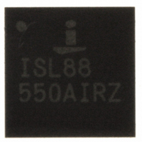
ISL88550AIRZ Intersil, ISL88550AIRZ Datasheet - Page 24

ISL88550AIRZ
Manufacturer Part Number
ISL88550AIRZ
Description
IC PWM CONTROLLER 28TQFN
Manufacturer
Intersil
Datasheet
1.ISL88550AIRZ.pdf
(25 pages)
Specifications of ISL88550AIRZ
Applications
PWM Controller
Voltage - Input
2 ~ 25 V
Current - Supply
25µA
Operating Temperature
-40°C ~ 85°C
Mounting Type
Surface Mount
Package / Case
28-TQFN
Rohs Compliant
YES
Lead Free Status / RoHS Status
Lead free / RoHS Compliant
Voltage - Supply
-
Available stocks
Company
Part Number
Manufacturer
Quantity
Price
Company:
Part Number:
ISL88550AIRZ
Manufacturer:
Intersil
Quantity:
480
Part Number:
ISL88550AIRZ
Manufacturer:
INTERSIL
Quantity:
20 000
Company:
Part Number:
ISL88550AIRZ-T
Manufacturer:
AMD
Quantity:
2
Part Number:
ISL88550AIRZ-T
Manufacturer:
INTERSIL
Quantity:
20 000
If the calculated V
minimum input voltage, then operating frequency must be
reduced or output capacitance added to obtain an
acceptable V
calculate V
A dropout design example is shown in Equation 36:
• V
• f
• K = 1.7µs
• t
• V
• h = 1.5
PC Board Layout Guidelines
Careful PC board layout is critical to achieve low switching
losses and clean, stable operation. The switching power
stage requires particular attention. If possible, mount all of
the power components on the topside of the board, with their
ground terminals flush against one another. Follow these
guidelines for good PC board layout:
• Keep the high-current paths short, especially at the
• Keep the power traces and load connections short. This
Intersil products are sold by description only. Intersil Corporation reserves the right to make changes in circuit design, software and/or specifications at any time without
notice. Accordingly, the reader is cautioned to verify that data sheets are current before placing orders. Information furnished by Intersil is believed to be accurate and
reliable. However, no responsibility is assumed by Intersil or its subsidiaries for its use; nor for any infringements of patents or other rights of third parties which may result
from its use. No license is granted by implication or otherwise under any patent or patent rights of Intersil or its subsidiaries.
V
IN
ground terminals. This practice is essential for stable,
jitter-free operation.
practice is essential for high efficiency. Using thick copper
PC boards (2oz vs 1oz) can enhance full-load efficiency
by 1% or more. Correctly routing PC board traces is a
difficult task that must be approached in terms of fractions
SW
OFF(MIN)
(
MIN
OUT
DROP1
)
=
= 600kHz
⎡
⎢
⎢
⎢
⎢
⎢
⎣
= 2.5V
1
−
2
SAG
⎛
⎜ ⎜
⎝
= V
5 .
1
= 450ns
SAG
5 .
V
1
DROP2
All Intersil U.S. products are manufactured, assembled and tested utilizing ISO9000 quality systems.
×
+
7 .
to be sure of adequate transient response.
450
0
µs
. If operation near dropout is anticipated,
1 .
IN(MIN)
V
ns
Intersil Corporation’s quality certifications can be viewed at www.intersil.com/design/quality
⎞
⎟ ⎟
⎠
⎤
⎥
⎥
⎥
⎥
⎥
⎦
= 100mV
For information regarding Intersil Corporation and its products, see www.intersil.com
+
0
is greater than the required
1 .
V
−
24
0
1 .
V
=
4
3 .
V
(EQ. 36)
ISL88550A
• Minimize current-sensing errors by connecting CSP and
• When trade-offs in trace lengths must be made, it is
• Route high-speed switching nodes (BOOT, PHASE,
Special Layout Considerations for LDO Section
The 20µF output capacitor (or capacitors) at VTT should be
placed as close to the VTT and PGND2 pins (pins 12 and
11) as possible to minimize the series resistance/inductance
in the trace. The PGND2 side of the capacitor should be
shorted with the lowest impedance path to the ground slug
underneath the IC, which should also be star-connected to
the GND (pin 24) of the IC. A narrower trace can be used to
tie the output voltage on the VTT side of the capacitor back
to the VTTS pin (pin 9). However, keep this trace well away
from noisy signals such as the PGND or PGND2 to prevent
noise from being injected into the error amplifier’s input. For
best performance, the VTTI bypass capacitor should also be
placed as close to the VTTI pin (pin 13) as possible. A short
low impedance connection should also be made to tie the
other side of the capacitor to the PGND2 pin. The REFIN pin
(pin 14) should be separately routed with a clean trace and
adequately bypass to AGND. A suggested layout of the
board can be found in the Evaluation Board Kit of
ISL88550A.
of centimeters, where a single m of excess trace
resistance causes a measurable efficiency penalty.
CSN directly across the current-sense resistor (R
preferable to allow the inductor-charging path to be made
longer than the discharge path. For example, it is better to
allow some extra distance between the input capacitors
and the high-side MOSFET than to allow distance
between the inductor and the low side MOSFET or
between the inductor and the output filter capacitor.
UGATE, and LGATE) away from sensitive analog areas
(REF, FB, and ILIM).
April 23, 2008
SENSE
FN6168.3
).


