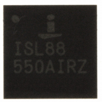
ISL88550AIRZ Intersil, ISL88550AIRZ Datasheet - Page 6

ISL88550AIRZ
Manufacturer Part Number
ISL88550AIRZ
Description
IC PWM CONTROLLER 28TQFN
Manufacturer
Intersil
Datasheet
1.ISL88550AIRZ.pdf
(25 pages)
Specifications of ISL88550AIRZ
Applications
PWM Controller
Voltage - Input
2 ~ 25 V
Current - Supply
25µA
Operating Temperature
-40°C ~ 85°C
Mounting Type
Surface Mount
Package / Case
28-TQFN
Rohs Compliant
YES
Lead Free Status / RoHS Status
Lead free / RoHS Compliant
Voltage - Supply
-
Available stocks
Company
Part Number
Manufacturer
Quantity
Price
Company:
Part Number:
ISL88550AIRZ
Manufacturer:
Intersil
Quantity:
480
Part Number:
ISL88550AIRZ
Manufacturer:
INTERSIL
Quantity:
20 000
Company:
Part Number:
ISL88550AIRZ-T
Manufacturer:
AMD
Quantity:
2
Part Number:
ISL88550AIRZ-T
Manufacturer:
INTERSIL
Quantity:
20 000
Pin Descriptions
PIN
10
12
13
14
15
16
17
18
11
1
2
3
4
5
6
7
8
9
OVP/UVP
PGND2
UGATE
STBY#
REFIN
NAME
POK1
POK2
VTTS
VTTR
TON
VTTI
OUT
REF
ILIM
VTT
VIN
SS
FB
6
t
to GND, REF, AV
t
t
t
t
Overvoltage/Undervoltage Protection Control Input. This four-level logic input enables or disables the
Overvoltage and/or Undervoltage Protection. The overvoltage limit is 116% of the nominal output voltage.
The undervoltage limit is 70% of the nominal output voltage. Discharge mode is enabled when OVP is also
enabled. Connect the OVP/UVP pin to the following pins for the desired function:
OVP/UVP = AV
OVP/UVP = OPEN (Enable OVP and discharge mode, disable UVP)
OVP/UVP = REF (Disable OVP and discharge mode, enable UVP)
OVP/UVP = GND (Disable OVP and discharge mode, disable UVP)
+2.0V Reference Voltage Output. Bypass to GND with a 0.1µF (min) bypass capacitor. REF can supply
50µA for external loads. Can be used for setting voltage for ILIM. REF turns off when SHDNA#, STBY# are
low.
Current-Limit Threshold Adjustment for Buck Regulator. The current-limit threshold across PGND and
PHASE is 0.1x the voltage at ILIM. Connect ILIM to a resistive-divider (typically from REF) to set the
current-limit threshold between 25mV and 200mV (with 0.25V to 2V at ILIM). Connect to AV
50mV default current-limit threshold.
Buck Power-Good Open-Drain Output. POK1 is low when the Buck output voltage is more than 10% above
or below the normal regulation point or during soft-start. POK1 is high impedance when the output is in
regulation and the soft-start circuit has terminated. POK1 is low in shutdown.
LDO Power-Good Open-Drain Output. In normal mode, POK2 is low when either VTTR or VTTS is more
than 10% above or below the normal regulation point, which is typically REFIN/2. In standby mode, POK2
responds only to VTTR input. POK2 is low in shutdown, and when VREFIN is less than 0.8V.
Stand-By Pin. Tie to low for low quiescent mode where the VTT output is disabled with high impedance but
the VTTR buffer is kept alive if SHDNA# is high. POK2 takes input from only VTTR in this mode. VTT is
discharged to 0V when SHDNA# = GND. PWM output can be on or off depending on the state of SHDNA#.
Soft-Start Control Pin for VTT and VTTR. Connect a capacitor (C
page 22) from SS to GND (see Soft-Start capacitor Selection in “LDO Section” on page 1). Leave SS open
to disable soft-start. SS discharged to GND when SHDNA# = GND
Sensing Pin for Termination Supply Output. Normally tied to VTT pin to allow accurate regulation to ½ the
REFIN voltage. Connected to a resistor divider from VTT to GND to regulate VTT to higher than ½ the
REFIN voltage.
Termination Reference Voltage. VTTR tracks the value of the VTT output.
Power Ground for the VTT and VTTR.
Termination Power Supply Output. Tie VTT to VTTS to regulate to V
Power Supply Input Voltage for VTT. Normally tied to output of buck regulator for DDR application.
External Reference Input. This is used to regulate the VTT and VTTR outputs to V
Feedback Input for Buck Output. Connect to GND for a +2.5V fixed output. For an adjustable output (0.7V
to 5.5V), connect FB to a resistive-divider from the output voltage. FB regulates to +0.7V.
Output Voltage Sense Connection. Connect directly to the positive terminal of the buck capacitors. OUT
senses the output voltage to determine the on-time for the high-side switching MOSFET (Q1 in the "Typical
Application Circuit" on page 22). OUT also serves as the buck output’s feedback input in fixed-output
modes. When discharge mode is enabled by OVP/UVP, the output capacitor is discharged through an
internal 20Ω resistor connected between OUT and ground.
Input Voltage Sense Connection. Connect to input power source. V
one-shot timer. This pin can range from 2V to 25V.
High-Side Gate-Driver Output. Swings from PHASE to BOOT. UGATE is low when in shutdown or UVLO.
ON
ON
ON
ON
ON
On-Time Selection-Control Input. This four-level logic input sets the nominal UGATE on-time. Connect
= AV
= OPEN (300kHz)
= REF (450kHz)
= GND (600kHz)
DD
(200kHz)
DD
DD
(Enable OVP and discharge mode, enable UVP)
, or leave t
ISL88550A
ON
unconnected to select the following nominal switching frequencies:
FUNCTION
9
in "Typical Application Circuit" on
IN
REFIN
is used only to set the PWM on-time
/2.
REFIN
/2
DD
to select the
April 23, 2008
FN6168.3


