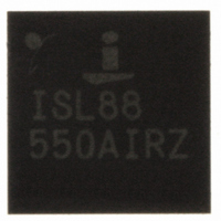
ISL88550AIRZ Intersil, ISL88550AIRZ Datasheet - Page 20

ISL88550AIRZ
Manufacturer Part Number
ISL88550AIRZ
Description
IC PWM CONTROLLER 28TQFN
Manufacturer
Intersil
Datasheet
1.ISL88550AIRZ.pdf
(25 pages)
Specifications of ISL88550AIRZ
Applications
PWM Controller
Voltage - Input
2 ~ 25 V
Current - Supply
25µA
Operating Temperature
-40°C ~ 85°C
Mounting Type
Surface Mount
Package / Case
28-TQFN
Rohs Compliant
YES
Lead Free Status / RoHS Status
Lead free / RoHS Compliant
Voltage - Supply
-
Available stocks
Company
Part Number
Manufacturer
Quantity
Price
Company:
Part Number:
ISL88550AIRZ
Manufacturer:
Intersil
Quantity:
480
Part Number:
ISL88550AIRZ
Manufacturer:
INTERSIL
Quantity:
20 000
Company:
Part Number:
ISL88550AIRZ-T
Manufacturer:
AMD
Quantity:
2
Part Number:
ISL88550AIRZ-T
Manufacturer:
INTERSIL
Quantity:
20 000
spuriously turn on because of dV/dt caused by high-side
MOSFET turning on, as this would result in shoot through
current degrading the efficiency. MOSFETs with a lower
Q
For proper thermal-management design, calculate the power
dissipation at the desired maximum operating junction
temperature, maximum output current, and worst-case input
voltage (for low-side MOSFET, worst case is at V
high-side MOSFET, it could be either at V
V
have different loss components due to the circuit operation.
The low-side MOSFET operates as a zero voltage switch;
therefore, major losses are:
P
where VF is the body-diode forward-voltage drop, t
dead time (~30ns), and f
Because of the zero-voltage switch operation, the low-side
MOSFET gate-drive loss occurs as a result of charging and
discharging the input capacitance, (CISS). This loss is
distributed among the average LGATE driver’s pull-up and
pull-down resistance, RLGATE (1Ω), and the internal gate
resistance (RGATE) of the MOSFET (~2Ω). The driver
power dissipated is given by Equation 18:
The high-side MOSFET operates as a duty-cycle control
switch and has the following major losses: the channel
conduction loss (P
(P
MOSFET does not have body-diode conduction loss
because the diode never conducts current:
Use r
where I
determined by Equation 21:
I
P
P
P
P
GATE
1. The channel conduction loss (P
2. The body diode conduction loss (P
3. The gate-drive loss (P
LSDC
IN(MAX)
LSCC
HSSW
GD
LSDR
HSCC
HSSW
( )
ON
=
=
to Q
DS(ON)
=
=
=
I 2
⎛
⎜ ⎜
⎝
C
V
GATE
V
=
1
LOAD
V
ISS
), and the drive loss (P
IN
OUT
−
R
). The high-side MOSFET and low-side MOSFET
IN
GS
×
V
UGATE
×
V
I
×
OUT
×
LOAD
V
IN
V
ratio have higher immunity to dV/dt.
at T
GS
I
is the average UGATE driver output-current
2
F
LOAD
5 .
⎞
⎟ ⎟
⎠
×
2
+
×
×
V
×
t
R
DT
J(MAX)
f
I
f
SW
SW
2
GATE
LOAD
HSCC
×
×
r
×
f
×
DS
SW
2
Q
R
×
(
ON
GS
r
GATE
.
I
DS
), the VI overlapping switching loss
GATE
SW
)
+
(
R
LSDR
ON
Q
GATE
+
)
GD
is the switching frequency.
R
20
LGATE
HSDR
)
LSCC
). The high-side
LSDC
)
IN(MIN)
)
IN(MAX)
or
DT
(EQ. 16)
(EQ. 17)
(EQ. 18)
(EQ. 19)
(EQ. 20)
(EQ. 21)
is the
; for
ISL88550A
where R
ON-resistance (1.5Ω typical) and R
resistance of the MOSFET (~2Ω):
where V
Equation 22, allow about 20% more for additional losses
because of MOSFET output capacitances and low-side
MOSFET body-diode reverse recovery charge dissipated in
the high-side MOSFET that is not well defined in the
MOSFET data sheet. Refer to the MOSFET data sheet for
thermal-resistance specifications to calculate the PC board
area needed to maintain the desired maximum operating
junction temperature with the above-calculated power
dissipations. To reduce EMI caused by switching noise, add
a 0.1µF ceramic capacitor from the high-side switch drain to
the low-side switch source, or add resistors in series with
UGATE and LGATE to slow down the switching transitions.
Adding series resistors increases the power dissipation of
the MOSFET, so ensure that this does not overheat the
MOSFET.
MOSFET Snubber Circuit (Buck)
Fast switching transitions cause ringing because of
resonating circuit parasitic inductance and capacitance at
the switching nodes. This high-frequency ringing occurs at
PHASE’s rising and falling transitions and can interfere with
circuit performance and generate EMI. A series R-C snubber
may be added across the lower MOSFET to dampen this
ringing. Following is the procedure for selecting the value of
the series RC circuit:
The circuit parasitic capacitance (C
equal to 1/3 the value of the added capacitance above. The
circuit parasitic inductance (L
Equation 23:
The resistor for critical dampening (R
2π × ƒR x L
the desired damping and the peak voltage excursion. The
capacitor (C
the C
snubber circuit (P
can be calculated as shown in Equation 24:
where V
frequency. Choose an R
specific application’s derating rule for the power dissipation
calculated.
P
L
P
1. Connect a scope probe to measure PHASE to GND, and
2. Find the capacitor value (connected from PHASE to
HSDR
PAR
RSNUB
observe the ringing frequency, f
GND) that reduces the ringing frequency by half.
=
PAR
=
(
=
2
Q
π
C
GS
IN
UGATE
G
×
SNUB
×
in order to be effective. The power loss of the
f
R
is the input voltage and f
V
PAR
= V
)
SNUB
1
GS
2
×
×
×
V
C
DD
. Adjust the resistor value up or down to tailor
IN
is the high-side MOSFET driver’s
f
PAR
SW
2
RSNUB
) should be at least 2x to 4x the value of
×
= 5V. In addition to the losses in
f
×
SW
R
GATE
SNUB
R
) is dissipated in the resistor and
GATE
+
R
UGATE
PAR
power rating that meets the
) is calculated using
GATE
PAR
SW
R
.
SNUB
) at PHASE is then
is the switching
is the internal gate
) is equal to
April 23, 2008
(EQ. 22)
(EQ. 23)
(EQ. 24)
FN6168.3


