C8051T600QDB Silicon Laboratories Inc, C8051T600QDB Datasheet - Page 98
C8051T600QDB
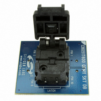
Manufacturer Part Number
C8051T600QDB
Description
BOARD SOCKET DAUGHTER QFN
Manufacturer
Silicon Laboratories Inc
Datasheet
1.C8051T600EDB.pdf
(188 pages)
Specifications of C8051T600QDB
Module/board Type
Socket Module - QFN
Data Bus Width
8 bit
Operating Supply Voltage
+ 1.8 V to + 3.6 V
Lead Free Status / RoHS Status
Contains lead / RoHS non-compliant
For Use With/related Products
C8051T600DK
Lead Free Status / Rohs Status
Lead free / RoHS Compliant
Other names
336-1406


C8051T600/1/2/3/4/5/6
20.1.2. EPROM Read Procedure
1. Reset the device using the RST pin.
2. Wait at least 20 µs before sending the first C2 command.
3. Place the device in core reset: Write 0x04 to the DEVCTL register.
4. Write 0x00 to the EPCTL register.
5. Write the first EPROM address for reading to EPADDRH and EPADDRL.
6. Read a data byte from EPDAT. EPADDRH:L will increment by 1 after this read.
7. (Optional) Check the ERROR bit in register EPSTAT and abort the memory read operation if necessary.
8. If reading is not finished, return to Step 6 to read the next address in sequence, or return to Step 5 to
9. Remove read mode (1st step): Write 0x40 to the EPCTL register.
10.Remove read mode (2nd step): Write 0x00 to the EPCTL register.
11. Reset the device: Write 0x02 and then 0x00 to the DEVCTL register.
20.2. Security Options
The C8051T600/1/2/3/4/5/6 devices provide security options to prevent unauthorized viewing of proprie-
tary program code and constants. A security byte in EPROM address space can be used to lock the pro-
gram memory from being read or written across the C2 interface. When read, the RDLOCK and WRLOCK
bits in register EPSTAT will indicate the lock status of the location currently addressed by EPADDR.
Table 20.1 shows the security byte decoding. See Section “15. Memory Organization” on page 74 for the
security byte location and EPROM memory map.
Important Note: Once the security byte has been written, there are no means of unlocking the
device. Locking memory from write access should be performed only after all other code has been
successfully programmed to memory.
98
select a new address.
Bits
7–4
3–0
Description
Write Lock: Clearing any of these bits to logic 0 prevents all code
memory from being written across the C2 interface.
Read Lock: Clearing any of these bits to logic 0 prevents all code
memory from being read across the C2 interface.
Table 20.1. Security Byte Decoding
Rev. 1.2
Related parts for C8051T600QDB
Image
Part Number
Description
Manufacturer
Datasheet
Request
R

Part Number:
Description:
SMD/C°/SINGLE-ENDED OUTPUT SILICON OSCILLATOR
Manufacturer:
Silicon Laboratories Inc
Part Number:
Description:
Manufacturer:
Silicon Laboratories Inc
Datasheet:
Part Number:
Description:
N/A N/A/SI4010 AES KEYFOB DEMO WITH LCD RX
Manufacturer:
Silicon Laboratories Inc
Datasheet:
Part Number:
Description:
N/A N/A/SI4010 SIMPLIFIED KEY FOB DEMO WITH LED RX
Manufacturer:
Silicon Laboratories Inc
Datasheet:
Part Number:
Description:
N/A/-40 TO 85 OC/EZLINK MODULE; F930/4432 HIGH BAND (REV E/B1)
Manufacturer:
Silicon Laboratories Inc
Part Number:
Description:
EZLink Module; F930/4432 Low Band (rev e/B1)
Manufacturer:
Silicon Laboratories Inc
Part Number:
Description:
I°/4460 10 DBM RADIO TEST CARD 434 MHZ
Manufacturer:
Silicon Laboratories Inc
Part Number:
Description:
I°/4461 14 DBM RADIO TEST CARD 868 MHZ
Manufacturer:
Silicon Laboratories Inc
Part Number:
Description:
I°/4463 20 DBM RFSWITCH RADIO TEST CARD 460 MHZ
Manufacturer:
Silicon Laboratories Inc
Part Number:
Description:
I°/4463 20 DBM RADIO TEST CARD 868 MHZ
Manufacturer:
Silicon Laboratories Inc
Part Number:
Description:
I°/4463 27 DBM RADIO TEST CARD 868 MHZ
Manufacturer:
Silicon Laboratories Inc
Part Number:
Description:
I°/4463 SKYWORKS 30 DBM RADIO TEST CARD 915 MHZ
Manufacturer:
Silicon Laboratories Inc
Part Number:
Description:
N/A N/A/-40 TO 85 OC/4463 RFMD 30 DBM RADIO TEST CARD 915 MHZ
Manufacturer:
Silicon Laboratories Inc
Part Number:
Description:
I°/4463 20 DBM RADIO TEST CARD 169 MHZ
Manufacturer:
Silicon Laboratories Inc