DK86065-2 Fujitsu Semiconductor America Inc, DK86065-2 Datasheet
DK86065-2
Specifications of DK86065-2


Related parts for DK86065-2


DK86065-2 Summary of contents
Page 1
Datasheet MB86065 14-bit 1+GSa/s DAC The Fujitsu MB86065 is a 14-bit 1+GSa/s digital to analog converter (DAC), delivering exceptional dynamic performance and backwards compatibility with ‘DAC A’ of the MB86064. The high performance DAC core is capable of generating multi- ...
Page 2
Contents 1 Functional Description . . . . . . . . . . . . . . . . . . . . . . . . . . . . . . . . . . . . ...
Page 3
September 2007 Version 1.01 FME/MS/DAC80S/DS/5344 MB86065 14-bit 1+GSa/s DAC 5.4 Ordering Information . . . . . . . . . . . . . . . . . . . . . . . . . . . . ...
Page 4
Functional Description The MB86065 is a high performance 14-bit 1+GSa/s DAC. In addition to the DAC core the device features a host of features designed to help both system integration and operation. A functional block diagram is shown in ...
Page 5
September 2007 Version 1.01 FME/MS/DAC80S/DS/5344 MB86065 14-bit 1+GSa/s DAC 1.1 Clock The device requires an input clock at half the DAC conversion rate, with sufficient spectral purity to not impact the target analog output performance. The DAC core is clocked ...
Page 6
DAC Core Clocks Programmable Delays The DAC core clocks contain programmable delays. These allow adjustment to the point at which data is clocked into the DAC core and when the analog portion of the DAC subsequently latches the data. ...
Page 7
September 2007 Version 1.01 FME/MS/DAC80S/DS/5344 MB86065 14-bit 1+GSa/s DAC 1.1.3 Waveform Memory Module Clock Programmable Delay A programmable delay stage is provided in the clock path prior to being applied to the Waveform Memory Module. This delay stage is programmed ...
Page 8
Table 5: Waveform Memory Module Register: WMM CONFIG [0x00] (Part Label 3 clkout1_cfg 0 0 clkout2_cfg 1 1 Also, programmable delay stages are provided in both CLK1_OUT and CLK2_OUT outputs. These clock output delays are programmed through ...
Page 9
September 2007 Version 1.01 FME/MS/DAC80S/DS/5344 MB86065 14-bit 1+GSa/s DAC 1.1.5 Loop Clock Maintaining valid clock-to-data timing becomes increasingly difficult at higher clock rates, particularly over tolerance with device-to-device variations. The MB86065 minimises potential problems through its DDR data interface and ...
Page 10
It is important not to adjust both delays simultaneously else they will counteract each other. Either the Clock Output delay or the Loop Clock delay, or both, should be zero. Connections to the loop clock are via pins LPCLK_IN and ...
Page 11
September 2007 Version 1.01 FME/MS/DAC80S/DS/5344 MB86065 14-bit 1+GSa/s DAC No Loop-Clock Low Typ. High FPGA 1.4V 1.5V 3.1V 3.3V DAC 1.6V 1.8V 2.9V 3.3V ...
Page 12
DAC Data The DAC core can be considered as two identical halves, referred to as ODD and EVEN. EVEN samples are latched on the falling edge of Clock Output, whilst ODD samples are latched on the rising edge. Data ...
Page 13
September 2007 Version 1.01 FME/MS/DAC80S/DS/5344 MB86065 14-bit 1+GSa/s DAC Table 10: Waveform Memory Module Register: WMM CONFIG [0x00] (Part WMM CONFIG Label (bit) 4 data_direct Port A data input 14-bit LVDS Port B data input 14-bit LVDS ...
Page 14
When using the Loop Clock, the delay set by loop_clk_dly (Table 8) opposes this and effectively advances the input data relative to the reference clock edge. Together these adjustments provide approximately 3ns trim range for clock-to-data timing, in 100ps steps. ...
Page 15
September 2007 Version 1.01 FME/MS/DAC80S/DS/5344 MB86065 14-bit 1+GSa/s DAC Table 11: DAC Core Register: DAC CONFIG [0x1C0] DAC CONFIG (bit DAC enabled 0 DAC disabled (default) 1.4 Voltage Reference A 1.2V bandgap reference is provided on-chip, although this ...
Page 16
DAC running at half the rate is much reduced sinx/x roll-off which gives increased output power and better in-band flatness when generating high output frequencies (e.g. 200MHz and above). This is illustrated in Figure 9 as line ...
Page 17
September 2007 Version 1.01 FME/MS/DAC80S/DS/5344 MB86065 14-bit 1+GSa/s DAC 1.7 Reset and Power Down Pin X_RESET is the device reset pin. On the falling edge of X_RESET the device is reset and all registers are set to their default values. ...
Page 18
Serial Control Interface A simple 4-wire serial control interface is used to control the MB86065. The serial interface uses pins SERIAL_IN, SERIAL_OUT, SERIAL_CLK and SERIAL_EN. Programmed settings are stored in a number of registers which are individually accessible using ...
Page 19
September 2007 Version 1.01 FME/MS/DAC80S/DS/5344 MB86065 14-bit 1+GSa/s DAC SERIAL_CLK Address SERIAL_IN msb Example of zero-filling a register SERIAL_EN SERIAL_OUT Figure 10 Serial Control Interface ‘Write’ Operation SERIAL_CLK SERIAL_IN msb Address SERIAL_EN SERIAL_OUT Figure 11 Serial Control Interface ‘Read’ Operation ...
Page 20
SERIAL_CLK SERIAL_IN & SERIAL_EN SERIAL_OUT Figure 12 Serial Control Interface Timing Requirements For initial testing & evaluation it is assumed that customers will use the Fujitsu PC USB Programming cable and software, both with the product development kit and for ...
Page 21
September 2007 Version 1.01 FME/MS/DAC80S/DS/5344 MB86065 14-bit 1+GSa/s DAC 3 Waveform Memory Module Enabling the Waveform Memory Module allows interleaving of LVDS data from both ports to drive the DAC core as well as access to any downloaded waveforms. The ...
Page 22
The data multiplexers are controlled by the WMM Registers, WMM [EVEN/ODD] MUX CTRL. Setting of these registers is referred to in the following two sections. Table 13: Waveform Memory Module Register: WMM [EVEN/ODD] MUX CTRL [0x11/0x21] WMM [EVEN/ ODD] MUX ...
Page 23
September 2007 Version 1.01 FME/MS/DAC80S/DS/5344 MB86065 14-bit 1+GSa/s DAC Remember to set register WMM CONFIG [0x00] bit data_direct to ‘1’ (see Table 10) The DAC will now sample both input ports, for consecutive DAC samples, as the EVEN and ODD ...
Page 24
RAM Access mux_a_ctrl[2] Controller mux_a_ctrl[3] mux_a_ctrl[2] RAM Access Controller Waveform Memory Module Figure 15 Waveform Memories Routing Diagram ODD and EVEN RAM elements within the module allow data to be routed to the ODD and EVEN phase DAC core data ...
Page 25
September 2007 Version 1.01 FME/MS/DAC80S/DS/5344 MB86065 14-bit 1+GSa/s DAC Table 17: Waveform Memory Module Registers: WMM [EVEN/ODD] RAM CTRL [0x12/0x22] WMM [EVEN/ ODD] RAM CTRL Label (bits) [10:0] prog_addr [21:11] prog_burst 22 prog_rw 23 prog_sel(1) 24 prog_sel(2) 25 prog_start When ...
Page 26
RAM A EVEN 0 32 prog_burst = prog_addr = 0 0 waveform samples.... Figure 16 Waveform Vector Storage in on-chip Memories prog_addr and prog_burst must be the same for RAM A ...
Page 27
September 2007 Version 1.01 FME/MS/DAC80S/DS/5344 MB86065 14-bit 1+GSa/s DAC data word received is not intended for that RAM element. A write sequence may be terminated early with a software reset (see section 3.3). The 64-bit wide WMM [EVEN/ODD] RAM DATA ...
Page 28
Programming the WMM / LVDS data source multiplexer bit ‘data_direct’ last will prevent incomplete and unsynchronised data reaching the DAC before it is required. 3.3 Software Reset The Waveform Memory Module may be reset through a software reset function. This ...
Page 29
September 2007 Version 1.01 FME/MS/DAC80S/DS/5344 MB86065 14-bit 1+GSa/s DAC 4 Electrical Characteristics 4.1 Absolute Maximum Ratings Parameter Supply voltage Analog supply Digital Supply Input Voltage LVDS inputs Digital control inputs Analog Output Voltage Analog Output Current Storage Temperature Junction Temperature ...
Page 30
DC Specifications Parameter DC Accuracy Integral Non Linearity Differential Non Linearity Analog output Full scale signal output current Current at each output Load resistance (single ended) Output resistance Output capacitance Gain error Output voltage (compliance) - Maximum Output voltage ...
Page 31
September 2007 Version 1.01 FME/MS/DAC80S/DS/5344 MB86065 14-bit 1+GSa/s DAC 4.4 AC Specifications Parameter Spurious-Free Dynamic Range Single tone at -1dBFS, 800MSa/ 400MHz 20 MHz 40 MHz 70 MHz 140 MHz 300 MHz Single tone at -1dBFS, 1GSa/s, DC ...
Page 32
Parameter (Continued) Adjacent Channel Leakage Ratio 1 x UMTS carrier, 5MHz channel spacing 30.72MHz centre frequency, 245.76MSa/s 276.48MHz centre frequency, 737.28MSa UMTS carriers, 5MHz channel spacing 276.48MHz centre frequency, 737.28MSa/s 414.72MHz centre frequency, 1105.92MSa/s Images Interleaved DAC image ...
Page 33
September 2007 Version 1.01 FME/MS/DAC80S/DS/5344 MB86065 14-bit 1+GSa/s DAC 4.6 Clock Specifications Parameter Clock Input Maximum clock frequency Clock frequency for 1+GSa/s mode Square Wave Low time High time Slew rate for minimum wide-band jitter Clock input duty cycle Low-level ...
Page 34
Serial Interface Timing Specifications Parameter Serial Clock Frequency Serial Clock Mark or Space Setup , SERIAL_IN to SERIAL_CLK rising edge Hold , SERIAL_IN from SERIAL_CLK rising edge Delay , SERIAL_CLK to SERIAL_OUT valid T (min (max), AVD33 ...
Page 35
September 2007 Version 1.01 FME/MS/DAC80S/DS/5344 MB86065 14-bit 1+GSa/s DAC 400 350 300 250 200 150 100 50 0 300 350 1,100 1,000 900 800 700 600 500 300 350 Copyright © 2004-2007 Fujitsu Microelectronics Europe GmbH Disclaimer : The contents ...
Page 36
Mechanical Data 5.1 Pin Assignment X_A9 X_A10 W23 W21 V22 A10 A9 V20 U23 U21 DVSS DVDD T20 X_A8 T22 X_A7 A8 A7 R23 R21 P20 P22 X_A6 X_A5 A6 N23 N21 A5 M22 DVSS DVDD M20 X_A3 X_A4 ...
Page 37
September 2007 Version 1.01 FME/MS/DAC80S/DS/5344 MB86065 14-bit 1+GSa/s DAC 5.2 Pin Definition Analog and Clock Interface Pin Nos. Pin Name D10, D14 AVD33 B16, A17 AVD18_A A7, B8 AVD18_B D12 AVD18_CLK C7, B12, C17 AVSS C15 IOUT D16 IOUTB C11 ...
Page 38
Digital Data Interface Pin Nos. Pin Name F2, F22, G1, M2, U1, DVDD AC7, AB12, AC17, U23, M22, G23 E1, E23, G3, M4, U3, DVSS AA7, Y12, AA17, U21, M20, G21 H20 A1 J21 X_A1 H22 A2 J23 X_A2 K20 ...
Page 39
September 2007 Version 1.01 FME/MS/DAC80S/DS/5344 MB86065 14-bit 1+GSa/s DAC Pin Nos. Pin Name L1 X_B4 X_B5 X_B6 X_B7 X_B8 X_B9 V4 B10 W3 X_B10 AA5 ...
Page 40
Package Data Dimensions in millimetres. Ball array viewed from below . Important: This device requires pre-baking at 125°C (257°F) for 24 hours before mounting unless removed from approved vacuum sealed packaging just prior to assembly. 5.4 Ordering Information The ...
Page 41
September 2007 Version 1.01 FME/MS/DAC80S/DS/5344 MB86065 14-bit 1+GSa/s DAC 6 Application Notes 6.1 PCB Power & Ground Plane Splits and Decoupling The following guidelines are suggestions to help obtain best performance from the MB86065. The information may be subject to ...
Page 42
CLKIN termination Pin 1 A: Top layer Pin 1 C: Internal layer 1 - IOUTB tracks (thick the termination resistors and CLKINB track (thin) Figure 19 Recommended PCB layout (All plots viewed from above) Production Page 42 of ...
Page 43
September 2007 Version 1.01 FME/MS/DAC80S/DS/5344 MB86065 14-bit 1+GSa/s DAC 6.2 Input Clock Interfacing The differential clock input to the device needs to be biased about the specified typical common mode input voltage. The exact interface circuitry will depend on the ...
Page 44
Clock Duty Cycle Optimisation Earlier sections of this data sheet document that the DAC core is clocked on both rising and falling edges of the input clock, and that a characteristic of this architecture is suppressed images of the ...
Page 45
September 2007 Version 1.01 FME/MS/DAC80S/DS/5344 MB86065 14-bit 1+GSa/s DAC 6.4 Analog Output Interfacing 6.4.1 Transformer Coupled Output Circuit The recommended analog output circuit is a two stage transformer circuit that provides both isolation from the analog ground plane and excellent ...
Page 46
necessary, the ground planes that the signals use as a reference plane must be linked together with vias next to the signal vias so that the return currents in the ground plane do not have to travel any distance away ...
Page 47
September 2007 Version 1.01 FME/MS/DAC80S/DS/5344 MB86065 14-bit 1+GSa/s DAC 6.5 Example Setup Register Settings The following sections provide examples of typical configurations for the MB86065 and required register settings. In all cases other registers are assumed their ...
Page 48
• {repeat above instruction 2045 times} • 0x13 0xXXXXXXX • 0x23 0xXXXXXXX • 0x22 0x27FF800 • 0x23 0xXXXXXXX • {repeat above instruction 2045 times} • 0x23 0xXXXXXXX • 0x12 0x0FFF800 • 0x22 0x0FFF800 • 0x11 0x30 • 0x21 0x30 • ...
Page 49
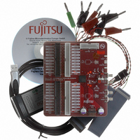
... MB86065 14-bit 1+GSa/s DAC 7 Development Kit A development kit, reference DK86065-2, is available for the MB86065 14-bit 1+GSa/s DAC. This comprises an evaluation board for the MB86065 and a PC programming cable with associated software. Connections for all analog signals are via SMA connectors, allowing instruments to be connected using standard cables. All digital I/O signals are routed to four 2-row 0.1” ...
Page 50
Using DKUSB-1 in Target Applications It is expected that customers can benefit from using Fujitsu’s PC USB Programming cable and accompanying PC software, DKUSB-1, for debug of prototype target applications. To facilitate recommended that an appropriate connector is fitted ...
Page 51
September 2007 Version 1.01 FME/MS/DAC80S/DS/5344 MB86065 14-bit 1+GSa/s DAC Appendix A Default Register Settings Appendix A.1 DAC Core Registers Register Address DAC 190 16 THOLD 01 1001 0000 DAC 191 16 SEED 01 1001 0001 ...
Page 52
Appendix A.2 Waveform Memory Module Registers Register Address WMM 00 16 CONFIG 000 0000 WMM EVEN 10 16 CONFIG 001 0000 WMM EVEN 11 16 MUX CTRL 001 0001 WMM EVEN 12 16 RAM CTRL 001 0010 WMM EVEN 13 ...
Page 53
September 2007 Version 1.01 FME/MS/DAC80S/DS/5344 MB86065 14-bit 1+GSa/s DAC Notes Copyright © 2004-2007 Fujitsu Microelectronics Europe GmbH Disclaimer : The contents of this document are subject to change without notice. Customers are advised to consult with FUJITSU sales representatives before ...
Page 54
Notes Production Page Disclaimer : The contents of this document are subject to change without notice. Customers are advised to consult with FUJITSU sales representatives before ordering.The information and circuit diagrams in this document are presented “as ...
Page 55
September 2007 Version 1.01 FME/MS/DAC80S/DS/5344 MB86065 14-bit 1+GSa/s DAC Notes Copyright © 2004-2007 Fujitsu Microelectronics Europe GmbH Disclaimer : The contents of this document are subject to change without notice. Customers are advised to consult with FUJITSU sales representatives before ...
Page 56
Worldwide Headquarters Japan Fujitsu Limited Tel: +81 44 754 3753 Fax: +81 44 754 3329 Kamikodanaka 4-1-1 Nakahara-ku Kawasaki-shi Kanagawa-ken 211-8588 Japan http://www.fujitsu.com USA Tel: +1 408 737 5600 Fujitsu Microelectronics America, Inc. Fax: +1 408 737 5999 1250 E. ...