DK86065-2 Fujitsu Semiconductor America Inc, DK86065-2 Datasheet - Page 37
DK86065-2
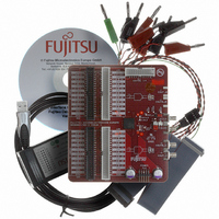
Manufacturer Part Number
DK86065-2
Description
KIT EVAL 16BIT DAC FOR MB86065
Manufacturer
Fujitsu Semiconductor America Inc
Specifications of DK86065-2
Number Of Dac's
1
Number Of Bits
14
Outputs And Type
1, Differential
Sampling Rate (per Second)
1G
Data Interface
Serial
Dac Type
Current
Voltage Supply Source
Analog and Digital
Operating Temperature
-40°C ~ 85°C
Utilized Ic / Part
MB86065
For Use With
865-1111 - DAC DK FPGA ADAPTER BOARD865-1012 - KIT DEV DUAL 14BIT MB86064 SMA
Lead Free Status / RoHS Status
Lead free / RoHS Compliant
Other names
865-1011


September 2007 Version 1.01
FME/MS/DAC80S/DS/5344
MB86065 14-bit 1+GSa/s DAC
5.2
Analog and Clock Interface
Thermal / Ground Array
Copyright © 2004-2007 Fujitsu Microelectronics Europe GmbH
Disclaimer : The contents of this document are subject to change without notice. Customers are advised to consult with FUJITSU sales representatives before
M13, M15, N10, N12,
K11, K13, K15, L10,
P15, R10, R12, R14
L12, L14, M9, M11,
N14, P9, P11, P13,
J10, J12, J14, K9,
C7, B12, C17
D10, D14
B16, A17
Pin Nos.
Pin Nos.
A7, B8
AC13
AB14
AC11
AB10
AA11
AA13
D12
C15
D16
C11
B10
C13
A15
A13
B14
Y10
Y14
A11
A9
Pin Definition
ordering.The information and circuit diagrams in this document are presented “as is”, no license is granted by implication or otherwise.
X_LPCLK_OUT
X_CLK1_OUT
X_CLK2_OUT
X_LPCLK_IN
LPCLK_OUT
AVD18_CLK
CLK1_OUT
CLK2_OUT
LPCLK_IN
Pin Name
Pin Name
AVD18_A
AVD18_B
CLKINB
VLO_A
VLO_B
AVD33
IOUTB
AVD25
CLKIN
BGAP
AVSS
VREF
RREF
IOUT
TG
Output
Output
Power
Power
Input/
Input/
O
O
O
O
O
O
O
O
O
O
O
O
O
O
O
O
-
I
I
I
I
I
Analog positive supply, +3.3V
DAC internal 1.8V regulator output
DAC internal 1.8V regulator output
Input clock internal 1.8V regulator output
Analog ground, 0V
DAC Positive Analog output
DAC Negative Analog output
Bandgap reference output
Voltage reference input
Analog output current reference resistor
Regulated 2.5V output (supply for external
voltage reference)
DAC clock reference level
DAC clock reference level
Clock input, positive input
Clock input, negative input
LVDS output clock #1, positive output
LVDS output clock #1, negative output
LVDS output clock #2, positive output
LVDS output clock #2, negative output
LVDS calibration loop clock, positive input
LVDS calibration loop clock, negative input
LVDS calibration loop clock, positive output
LVDS calibration loop clock, negative output
Thermal / Ground array connection
Description
Description
Production
Decouple to AVSS
Decouple to AVSS
Decouple to AVSS
Decouple to AVSS
Refer to section 1.4
Refer to section 1.4
Refer to section 1.5
Decouple to AVSS
Decouple to AVD18_A
Decouple to AVD18_B
Requires biasing
Use double termination
Use double termination
Use double termination
Connect to the DVSS digital
ground plane
- Refer to section 6.2
Note
Note
Page 37 of 56
Related parts for DK86065-2
Image
Part Number
Description
Manufacturer
Datasheet
Request
R

Part Number:
Description:
IC POWER SUPPLY MONITOR 8SOP
Manufacturer:
Fujitsu Semiconductor America Inc
Datasheet:
Part Number:
Description:
IC POWER SUPPLY MONITOR 8SOP
Manufacturer:
Fujitsu Semiconductor America Inc
Datasheet:

Part Number:
Description:
IC MCU 60K FLASH 2KB RAM 52LQFP
Manufacturer:
Fujitsu Semiconductor America Inc
Datasheet:

Part Number:
Description:
IC MCU 32BIT 256KB FLASH 120LQFP
Manufacturer:
Fujitsu Semiconductor America Inc
Datasheet:
Part Number:
Description:
IC CTLR TOUCH SENSOR 12CH 30SSOP
Manufacturer:
Fujitsu Semiconductor America Inc
Datasheet:

Part Number:
Description:
IC CTLR TOUCH SENSOR 12CH 40QFN
Manufacturer:
Fujitsu Semiconductor America Inc
Datasheet:
Part Number:
Description:
SYNTHESIZER PLL DUAL INP 20SSOP
Manufacturer:
Fujitsu Semiconductor America Inc
Datasheet:

Part Number:
Description:
SYNTHESZR PLL 1.1GHZ DUAL 16SSOP
Manufacturer:
Fujitsu Semiconductor America Inc
Datasheet:

Part Number:
Description:
IC SSCG EMI RED 8-SOIC
Manufacturer:
Fujitsu Semiconductor America Inc
Datasheet:

Part Number:
Description:
IC SSCG EMI RED 8-TSSOP
Manufacturer:
Fujitsu Semiconductor America Inc
Datasheet:

Part Number:
Description:
IC SSCG EMI RED 8-SOP
Manufacturer:
Fujitsu Semiconductor America Inc
Datasheet:

Part Number:
Description:
SYNTHESIZER PLL 2.5GHZ 16SSOP
Manufacturer:
Fujitsu Semiconductor America Inc
Datasheet:
Part Number:
Description:
SYNTHESIZER PLL 1.2GHZ 16SSOP
Manufacturer:
Fujitsu Semiconductor America Inc
Datasheet:

Part Number:
Description:
SYNTHESIZER PLL 2.5GHZ 16BCC
Manufacturer:
Fujitsu Semiconductor America Inc
Datasheet:

Part Number:
Description:
IC SSCG EMI RED 8-SOP
Manufacturer:
Fujitsu Semiconductor America Inc
Datasheet: