DK86065-2 Fujitsu Semiconductor America Inc, DK86065-2 Datasheet - Page 27
DK86065-2
Manufacturer Part Number
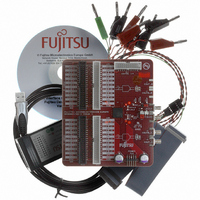
DK86065-2
Description
KIT EVAL 16BIT DAC FOR MB86065
Manufacturer
Fujitsu Semiconductor America Inc
Specifications of DK86065-2
Number Of Dac's
1
Number Of Bits
14
Outputs And Type
1, Differential
Sampling Rate (per Second)
1G
Data Interface
Serial
Dac Type
Current
Voltage Supply Source
Analog and Digital
Operating Temperature
-40°C ~ 85°C
Utilized Ic / Part
MB86065
For Use With
865-1111 - DAC DK FPGA ADAPTER BOARD865-1012 - KIT DEV DUAL 14BIT MB86064 SMA
Lead Free Status / RoHS Status
Lead free / RoHS Compliant
Other names
865-1011


September 2007 Version 1.01
FME/MS/DAC80S/DS/5344
MB86065 14-bit 1+GSa/s DAC
data word received is not intended for that RAM element. A write sequence may be terminated early
with a software reset (see section 3.3).
The 64-bit wide WMM [EVEN/ODD] RAM DATA registers are used to transfer pre-formatted data into
the RAM address location selected by the RAM Access Controller. See Table 18. The 14-bit DAC
data should be MSB aligned to the 15th bit of the waveform sample (DAC data D14 aligned to
waveform bit 14 [15:0], i.e. register bits 0, 15, 16, 31, 32, 47, 48, 63 etc. are not used).
The following sequence could be followed,
• write the first pre-formatted RAM data word to register WMM EVEN RAM DATA
• write to register WMM EVEN RAM CTRL with bit prog_start set
• consecutively write the remaining RAM data words to register WMM EVEN RAM DATA.
Once the RAM Access Controller returns to the idle state, after a successful write sequence, data
transfer starts automatically. However, until the other RAM element is programmed and the RAMs
are synchronised, the output sequence will be corrupt.
• repeat the above sequence for the ODD RAM element.
The order in which the EVEN/ODD RAMs are programmed is not important.
Once all of the required RAMs have been programmed, the RAM Access Controllers need to be set
to ‘run’ and synchronised by a software reset, see Section 3.3. Finally, ensure that all ODD, EVEN
and the WMM/LVDS data multiplexers are set appropriately. A worked example is given in section
6.5.3
Copyright © 2004-2007 Fujitsu Microelectronics Europe GmbH
Disclaimer : The contents of this document are subject to change without notice. Customers are advised to consult with FUJITSU sales representatives before
Table 18: Waveform Memory Module Registers: WMM [EVEN/ODD] RAM DATA [0x13/0x23]
WMM EVEN RAM
WMM ODD RAM
DATA
DATA
[31:16]
[47:32]
[63:48]
[31:16]
[47:32]
[63:48]
ordering.The information and circuit diagrams in this document are presented “as is”, no license is granted by implication or otherwise.
(bits)
(bits)
[15:0]
[15:0]
prog_data
prog_data
Label
Label
Waveform EVEN sample word n
Waveform EVEN sample word n+2
Waveform EVEN sample word n+4
Waveform EVEN sample word n+6
Waveform ODD sample word n+1
Waveform ODD sample word n+3
Waveform ODD sample word n+5
Waveform ODD sample word n+7
Function
Function
Production
Page 27 of 56
Related parts for DK86065-2
Image
Part Number
Description
Manufacturer
Datasheet
Request
R

Part Number:
Description:
IC POWER SUPPLY MONITOR 8SOP
Manufacturer:
Fujitsu Semiconductor America Inc
Datasheet:
Part Number:
Description:
IC POWER SUPPLY MONITOR 8SOP
Manufacturer:
Fujitsu Semiconductor America Inc
Datasheet:

Part Number:
Description:
IC MCU 60K FLASH 2KB RAM 52LQFP
Manufacturer:
Fujitsu Semiconductor America Inc
Datasheet:

Part Number:
Description:
IC MCU 32BIT 256KB FLASH 120LQFP
Manufacturer:
Fujitsu Semiconductor America Inc
Datasheet:
Part Number:
Description:
IC CTLR TOUCH SENSOR 12CH 30SSOP
Manufacturer:
Fujitsu Semiconductor America Inc
Datasheet:

Part Number:
Description:
IC CTLR TOUCH SENSOR 12CH 40QFN
Manufacturer:
Fujitsu Semiconductor America Inc
Datasheet:
Part Number:
Description:
SYNTHESIZER PLL DUAL INP 20SSOP
Manufacturer:
Fujitsu Semiconductor America Inc
Datasheet:

Part Number:
Description:
SYNTHESZR PLL 1.1GHZ DUAL 16SSOP
Manufacturer:
Fujitsu Semiconductor America Inc
Datasheet:

Part Number:
Description:
IC SSCG EMI RED 8-SOIC
Manufacturer:
Fujitsu Semiconductor America Inc
Datasheet:

Part Number:
Description:
IC SSCG EMI RED 8-TSSOP
Manufacturer:
Fujitsu Semiconductor America Inc
Datasheet:

Part Number:
Description:
IC SSCG EMI RED 8-SOP
Manufacturer:
Fujitsu Semiconductor America Inc
Datasheet:

Part Number:
Description:
SYNTHESIZER PLL 2.5GHZ 16SSOP
Manufacturer:
Fujitsu Semiconductor America Inc
Datasheet:
Part Number:
Description:
SYNTHESIZER PLL 1.2GHZ 16SSOP
Manufacturer:
Fujitsu Semiconductor America Inc
Datasheet:

Part Number:
Description:
SYNTHESIZER PLL 2.5GHZ 16BCC
Manufacturer:
Fujitsu Semiconductor America Inc
Datasheet:

Part Number:
Description:
IC SSCG EMI RED 8-SOP
Manufacturer:
Fujitsu Semiconductor America Inc
Datasheet: