DK86065-2 Fujitsu Semiconductor America Inc, DK86065-2 Datasheet - Page 18
DK86065-2
Manufacturer Part Number
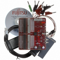
DK86065-2
Description
KIT EVAL 16BIT DAC FOR MB86065
Manufacturer
Fujitsu Semiconductor America Inc
Specifications of DK86065-2
Number Of Dac's
1
Number Of Bits
14
Outputs And Type
1, Differential
Sampling Rate (per Second)
1G
Data Interface
Serial
Dac Type
Current
Voltage Supply Source
Analog and Digital
Operating Temperature
-40°C ~ 85°C
Utilized Ic / Part
MB86065
For Use With
865-1111 - DAC DK FPGA ADAPTER BOARD865-1012 - KIT DEV DUAL 14BIT MB86064 SMA
Lead Free Status / RoHS Status
Lead free / RoHS Compliant
Other names
865-1011


2
A simple 4-wire serial control interface is used to control the MB86065. The serial interface uses pins
SERIAL_IN, SERIAL_OUT, SERIAL_CLK and SERIAL_EN. Programmed settings are stored in a
number of registers which are individually accessible using either an 7-bit (WMM Registers) or 10-bit
(DAC Core Registers) address/control word. Data may be written to or read from each of these
registers.
2.1
To perform a read or write cycle SERIAL_EN should be taken high on the falling edge of
SERIAL_CLK. This will indicate the start of a frame when latched on the next rising edge. At the same
time SERIAL_IN should be driven, MSB first, with the address of the register to be accessed. Data
is latched into the device on each rising edge of SERIAL_CLK. The register address should be
followed with the read/write instruction bit. For a read cycle this bit is ‘0’, for a write cycle this bit is ‘1’.
The device is now ready to transfer data in or out of the addressed register.
If the selected register is to be written to, the data should be presented to SERIAL_IN, MSB first. The
data packet only needs to be as long as the register that is being written to, with the LSB presented
in the final time slot. If the data source has a fixed length packet size, longer than the register, the
data packet should be zero-filled at the MSB end. Once the data has been transferred into the
register, SERIAL_EN should be taken low on the falling edge of SERIAL_CLK to indicate the end of
the read/write cycle and frame. During a write cycle, as data is loaded into the selected register, the
previous contents are output on SERIAL_OUT, MSB first.
If the selected register is being read, data will be output on SERIAL_OUT, MSB first, nominally
coincident with the falling edge of SERIAL_CLK. Once the register has been read additional clock
cycles will produce zero-filled bits until the read cycle is terminated. A read cycle may be terminated
by taking the SERIAL_EN low on the falling edge of SERIAL_CLK.
Figure 10 and Figure 11 show the write and read cycles (as functional timing diagrams) in more
detail.
Page 18 of 56
Disclaimer : The contents of this document are subject to change without notice. Customers are advised to consult with FUJITSU sales representatives before
Serial Control Interface
Programming a Read/Write Cycle
ordering.The information and circuit diagrams in this document are presented “as is”, no license is granted by implication or otherwise.
The serial interface uses 1.8V LV-CMOS logic levels.
All Waveform Memory Module registers, apart from WMM [EVEN/ODD] RAM DATA, read
back as eight bit long registers. All other registers will read back at their true length.
In designs where SERIAL_CLK is halted after a Write operation, at least three additional
clock cycles should be allowed after SERIAL_EN has return low. This is necessary to
complete the internal register programming.
Production
Copyright © 2004-2007 Fujitsu Microelectronics Europe GmbH
MB86065 14-bit 1+GSa/s DAC
September 2007 Version 1.01
FME/MS/DAC80S/DS/5344
Related parts for DK86065-2
Image
Part Number
Description
Manufacturer
Datasheet
Request
R

Part Number:
Description:
IC POWER SUPPLY MONITOR 8SOP
Manufacturer:
Fujitsu Semiconductor America Inc
Datasheet:
Part Number:
Description:
IC POWER SUPPLY MONITOR 8SOP
Manufacturer:
Fujitsu Semiconductor America Inc
Datasheet:

Part Number:
Description:
IC MCU 60K FLASH 2KB RAM 52LQFP
Manufacturer:
Fujitsu Semiconductor America Inc
Datasheet:

Part Number:
Description:
IC MCU 32BIT 256KB FLASH 120LQFP
Manufacturer:
Fujitsu Semiconductor America Inc
Datasheet:
Part Number:
Description:
IC CTLR TOUCH SENSOR 12CH 30SSOP
Manufacturer:
Fujitsu Semiconductor America Inc
Datasheet:

Part Number:
Description:
IC CTLR TOUCH SENSOR 12CH 40QFN
Manufacturer:
Fujitsu Semiconductor America Inc
Datasheet:
Part Number:
Description:
SYNTHESIZER PLL DUAL INP 20SSOP
Manufacturer:
Fujitsu Semiconductor America Inc
Datasheet:

Part Number:
Description:
SYNTHESZR PLL 1.1GHZ DUAL 16SSOP
Manufacturer:
Fujitsu Semiconductor America Inc
Datasheet:

Part Number:
Description:
IC SSCG EMI RED 8-SOIC
Manufacturer:
Fujitsu Semiconductor America Inc
Datasheet:

Part Number:
Description:
IC SSCG EMI RED 8-TSSOP
Manufacturer:
Fujitsu Semiconductor America Inc
Datasheet:

Part Number:
Description:
IC SSCG EMI RED 8-SOP
Manufacturer:
Fujitsu Semiconductor America Inc
Datasheet:

Part Number:
Description:
SYNTHESIZER PLL 2.5GHZ 16SSOP
Manufacturer:
Fujitsu Semiconductor America Inc
Datasheet:
Part Number:
Description:
SYNTHESIZER PLL 1.2GHZ 16SSOP
Manufacturer:
Fujitsu Semiconductor America Inc
Datasheet:

Part Number:
Description:
SYNTHESIZER PLL 2.5GHZ 16BCC
Manufacturer:
Fujitsu Semiconductor America Inc
Datasheet:

Part Number:
Description:
IC SSCG EMI RED 8-SOP
Manufacturer:
Fujitsu Semiconductor America Inc
Datasheet: