DK86065-2 Fujitsu Semiconductor America Inc, DK86065-2 Datasheet - Page 25
DK86065-2
Manufacturer Part Number
DK86065-2
Description
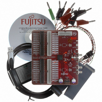
KIT EVAL 16BIT DAC FOR MB86065
Manufacturer
Fujitsu Semiconductor America Inc
Specifications of DK86065-2
Number Of Dac's
1
Number Of Bits
14
Outputs And Type
1, Differential
Sampling Rate (per Second)
1G
Data Interface
Serial
Dac Type
Current
Voltage Supply Source
Analog and Digital
Operating Temperature
-40°C ~ 85°C
Utilized Ic / Part
MB86065
For Use With
865-1111 - DAC DK FPGA ADAPTER BOARD865-1012 - KIT DEV DUAL 14BIT MB86064 SMA
Lead Free Status / RoHS Status
Lead free / RoHS Compliant
Other names
865-1011


September 2007 Version 1.01
FME/MS/DAC80S/DS/5344
MB86065 14-bit 1+GSa/s DAC
The WMM [EVEN/ODD] RAM CTRL registers prog_addr fields are used to define the start address
of the waveform. These fields should be set to 0 in order to store a full 16k point waveform. For the
multiple waveform mode, the number entered into these fields is the start location within the 2k x 64-
bit ODD/EVEN RAM element that the waveform is to be stored. One address location in this field
translates to eight waveform vector points because four points are stored at each address of the ODD
and EVEN RAM blocks.
The WMM [EVEN/ODD] RAM CTRL registers prog_burst fields sets the length of the stored
waveform, defined as the number of waveform points divided by eight, minus one. Every RAM
address in each of the ODD, EVEN, RAM A and RAM B memories corresponds to a 64-bit location.
Each location is divided into four 16-bit samples.
Figure 16 shows an example of how a 32 point vector is stored. In this example prog_addr is set to
0 and prog_burst = 3.
Copyright © 2004-2007 Fujitsu Microelectronics Europe GmbH
Disclaimer : The contents of this document are subject to change without notice. Customers are advised to consult with FUJITSU sales representatives before
Table 17: Waveform Memory Module Registers: WMM [EVEN/ODD] RAM CTRL [0x12/0x22]
ODD] RAM CTRL
WMM [EVEN/
[21:11]
ordering.The information and circuit diagrams in this document are presented “as is”, no license is granted by implication or otherwise.
(bits)
[10:0]
When programming the WMM on-chip memories ensure that the Clock Input (f
greater than 16 times the serial interface clock frequency (f
22
23
24
25
prog_sel(1)
prog_sel(2)
prog_burst
prog_addr
prog_start
prog_rw
Label
RAM access start address
RAM access burst size
Access burst size should be programmed as ((No. of points/8) - 1)
A value of zero indicates a single word access
RAM serial interface access mode
0 = Read mode (default)
1 = Write mode
RAM write select (1). Dependent on prog_sel(2) setting
0 = Write data to RAM A (default)
1 = Write data to RAM B
RAM write select (2)
0 = prog_sel(1) operates as normal (default)
1 = Writes the same data to both RAM A and RAM B
RAM Access Controller control
0 = Cycle through vector address range (default)
1 = Program RAMs
This bit is self clearing
Function
Production
sclk
) for correct operation.
Page 25 of 56
Clk
) is
Related parts for DK86065-2
Image
Part Number
Description
Manufacturer
Datasheet
Request
R

Part Number:
Description:
IC POWER SUPPLY MONITOR 8SOP
Manufacturer:
Fujitsu Semiconductor America Inc
Datasheet:
Part Number:
Description:
IC POWER SUPPLY MONITOR 8SOP
Manufacturer:
Fujitsu Semiconductor America Inc
Datasheet:

Part Number:
Description:
IC MCU 60K FLASH 2KB RAM 52LQFP
Manufacturer:
Fujitsu Semiconductor America Inc
Datasheet:

Part Number:
Description:
IC MCU 32BIT 256KB FLASH 120LQFP
Manufacturer:
Fujitsu Semiconductor America Inc
Datasheet:
Part Number:
Description:
IC CTLR TOUCH SENSOR 12CH 30SSOP
Manufacturer:
Fujitsu Semiconductor America Inc
Datasheet:

Part Number:
Description:
IC CTLR TOUCH SENSOR 12CH 40QFN
Manufacturer:
Fujitsu Semiconductor America Inc
Datasheet:
Part Number:
Description:
SYNTHESIZER PLL DUAL INP 20SSOP
Manufacturer:
Fujitsu Semiconductor America Inc
Datasheet:

Part Number:
Description:
SYNTHESZR PLL 1.1GHZ DUAL 16SSOP
Manufacturer:
Fujitsu Semiconductor America Inc
Datasheet:

Part Number:
Description:
IC SSCG EMI RED 8-SOIC
Manufacturer:
Fujitsu Semiconductor America Inc
Datasheet:

Part Number:
Description:
IC SSCG EMI RED 8-TSSOP
Manufacturer:
Fujitsu Semiconductor America Inc
Datasheet:

Part Number:
Description:
IC SSCG EMI RED 8-SOP
Manufacturer:
Fujitsu Semiconductor America Inc
Datasheet:

Part Number:
Description:
SYNTHESIZER PLL 2.5GHZ 16SSOP
Manufacturer:
Fujitsu Semiconductor America Inc
Datasheet:
Part Number:
Description:
SYNTHESIZER PLL 1.2GHZ 16SSOP
Manufacturer:
Fujitsu Semiconductor America Inc
Datasheet:

Part Number:
Description:
SYNTHESIZER PLL 2.5GHZ 16BCC
Manufacturer:
Fujitsu Semiconductor America Inc
Datasheet:

Part Number:
Description:
IC SSCG EMI RED 8-SOP
Manufacturer:
Fujitsu Semiconductor America Inc
Datasheet: