DK86065-2 Fujitsu Semiconductor America Inc, DK86065-2 Datasheet - Page 46
DK86065-2
Manufacturer Part Number
DK86065-2
Description
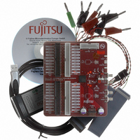
KIT EVAL 16BIT DAC FOR MB86065
Manufacturer
Fujitsu Semiconductor America Inc
Specifications of DK86065-2
Number Of Dac's
1
Number Of Bits
14
Outputs And Type
1, Differential
Sampling Rate (per Second)
1G
Data Interface
Serial
Dac Type
Current
Voltage Supply Source
Analog and Digital
Operating Temperature
-40°C ~ 85°C
Utilized Ic / Part
MB86065
For Use With
865-1111 - DAC DK FPGA ADAPTER BOARD865-1012 - KIT DEV DUAL 14BIT MB86064 SMA
Lead Free Status / RoHS Status
Lead free / RoHS Compliant
Other names
865-1011


necessary, the ground planes that the signals use as a reference plane must be linked together with
vias next to the signal vias so that the return currents in the ground plane do not have to travel any
distance away from the signal tracks when switching ground layers.
The RCR network, shown in Figure 22, is to compensate for the ADT1-1WT transformer becoming
inductive at high frequencies. The 10pF capacitor can be replaced with a variable capacitor to allow
optimisation of overshoot at the transformer input. However, this may not be required in all instances,
particularly frequency domain applications, since it increases in-band roll-off. For direct-IF, bandpass
applications it may be possible to tune out the DAC’s output capacitance, Cout, by resonating it with
a parallel inductor. For example, about 16nH to GND at each output or 33nH between the outputs for
a ~270MHz IF (assuming ideal resistive load). The ADTL1-4-75 transmission line transformer may
be removed to simplify the circuit, but this will reduce high frequency rejection of common-mode
noise and may reduce system performance in some applications.
6.4.2 Direct Interface to Quadrature Modulator
Some applications require a DC shift in order to interface the DAC output directly to components such
as a quadrature modulator. Traditionally this is not an easy challenge without impacting noise and
distortion. However, it may be possible to achieve the optimum operating point of both components
by off-setting supply rails/domains. For example, consider a modulator that normally runs on a +5V
supply and requires a +1.5V DC bias at its baseband inputs. Whereas the optimum DC bias at the
DAC output (for maximum signal swing) is -0.3V.
By shifting the modulator supply to operate between +3.3V (already needed for the DAC) and -1.8V
(at all GND pins) supplies, providing a total and acceptable 5.1V supply, all that is needed is
appropriate termination resistors at the DAC output, split between 0V and -1.8V, to give the correct
-0.3V DC bias at the DAC output and meet the optimal +1.5V DC bias, relative to its VSS pins, at the
modulator input.
Page 46 of 56
Disclaimer : The contents of this document are subject to change without notice. Customers are advised to consult with FUJITSU sales representatives before
ordering.The information and circuit diagrams in this document are presented “as is”, no license is granted by implication or otherwise.
MB86064
For either higher impedance or DC coupled loads it is important to note that the output
voltage compliance range for best performance is symmetrical about -0.3V not 0V.
AVD33
IOUTB
AVSS
IOUT
Figure 23 Suggested Direct Interface to Quadrature Modulator
AVSS
+3.3V
50R
50R
Production
-0.3V (DC)
-0.3V (DC)
Copyright © 2004-2007 Fujitsu Microelectronics Europe GmbH
AVSS
MB86065 14-bit 1+GSa/s DAC
50R
50R
September 2007 Version 1.01
+3.3V
-1.8V
10R
-1.8V
FME/MS/DAC80S/DS/5344
VDD
IN_P
IN_N
VSS
Quadrature
Modulator
Related parts for DK86065-2
Image
Part Number
Description
Manufacturer
Datasheet
Request
R

Part Number:
Description:
IC POWER SUPPLY MONITOR 8SOP
Manufacturer:
Fujitsu Semiconductor America Inc
Datasheet:
Part Number:
Description:
IC POWER SUPPLY MONITOR 8SOP
Manufacturer:
Fujitsu Semiconductor America Inc
Datasheet:

Part Number:
Description:
IC MCU 60K FLASH 2KB RAM 52LQFP
Manufacturer:
Fujitsu Semiconductor America Inc
Datasheet:

Part Number:
Description:
IC MCU 32BIT 256KB FLASH 120LQFP
Manufacturer:
Fujitsu Semiconductor America Inc
Datasheet:
Part Number:
Description:
IC CTLR TOUCH SENSOR 12CH 30SSOP
Manufacturer:
Fujitsu Semiconductor America Inc
Datasheet:

Part Number:
Description:
IC CTLR TOUCH SENSOR 12CH 40QFN
Manufacturer:
Fujitsu Semiconductor America Inc
Datasheet:
Part Number:
Description:
SYNTHESIZER PLL DUAL INP 20SSOP
Manufacturer:
Fujitsu Semiconductor America Inc
Datasheet:

Part Number:
Description:
SYNTHESZR PLL 1.1GHZ DUAL 16SSOP
Manufacturer:
Fujitsu Semiconductor America Inc
Datasheet:

Part Number:
Description:
IC SSCG EMI RED 8-SOIC
Manufacturer:
Fujitsu Semiconductor America Inc
Datasheet:

Part Number:
Description:
IC SSCG EMI RED 8-TSSOP
Manufacturer:
Fujitsu Semiconductor America Inc
Datasheet:

Part Number:
Description:
IC SSCG EMI RED 8-SOP
Manufacturer:
Fujitsu Semiconductor America Inc
Datasheet:

Part Number:
Description:
SYNTHESIZER PLL 2.5GHZ 16SSOP
Manufacturer:
Fujitsu Semiconductor America Inc
Datasheet:
Part Number:
Description:
SYNTHESIZER PLL 1.2GHZ 16SSOP
Manufacturer:
Fujitsu Semiconductor America Inc
Datasheet:

Part Number:
Description:
SYNTHESIZER PLL 2.5GHZ 16BCC
Manufacturer:
Fujitsu Semiconductor America Inc
Datasheet:

Part Number:
Description:
IC SSCG EMI RED 8-SOP
Manufacturer:
Fujitsu Semiconductor America Inc
Datasheet: