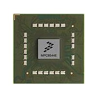
MPC8544DS Freescale Semiconductor, MPC8544DS Datasheet - Page 91

MPC8544DS
Manufacturer Part Number
MPC8544DS
Description
BOARD DEVELOPMENT SYSTEM 8544
Manufacturer
Freescale Semiconductor
Series
PowerQUICC III™r
Type
MPUr
Datasheets
1.MPC8544VTALF.pdf
(117 pages)
2.MPC8544VTALF.pdf
(2 pages)
3.MPC8544VTALF.pdf
(1340 pages)
4.MPC8544DS.pdf
(2 pages)
Specifications of MPC8544DS
Contents
Board
Processor To Be Evaluated
MPC8544E
Data Bus Width
32 bit
Interface Type
Ethernet, I2C
Operating Supply Voltage
- 0.3 V to + 1.1 V
Leaded Process Compatible
Yes
Peak Reflow Compatible (260 C)
Yes
Rohs Compliant
Yes
For Use With/related Products
MPC8544
For Use With
PPC8544EVTANG - EVAL MPC8544 783FCPBGA
Lead Free Status / RoHS Status
Lead free / RoHS Compliant
Freescale Semiconductor
AVDD_SRDS
AVDD_SRDS2
SENSEVDD
SENSEVSS
MVREF
SD1_IMP_CAL_RX
SD1_IMP_CAL_TX
SD1_PLL_TPA
SD2_IMP_CAL_RX
SD2_IMP_CAL_TX
SD2_PLL_TPA
NC
Notes:
5. Treat these pins as no connects (NC) unless using debug address functionality.
1.All multiplexed signals are listed only once and do not re-occur. For example, LCS5/DMA_REQ2 is listed only once in the
2.Recommend a weak pull-up resistor (2–10 KΩ) be placed on this pin to OV
3.This pin must always be pulled high.
4.This pin is a reset configuration pin. It has a weak internal pull-up P-FET which is enabled only when the processor is in the
Local Bus Controller Interface section, and is not mentioned in the DMA section even though the pin also functions as
DMA_REQ2.
reset state. This pull-up is designed such that it can be overpowered by an external 4.7-kΩ pull-down resistor. However, if
the signal is intended to be high after reset, and if there is any device on the net which might pull down the value of the net
at reset, then a pull-up or active driver is needed. TSEC3_TXD[3] (cfg_srds_sgmii_refclk) is an exception, because the
default value of this configuration signal is low (0). Thus, no external pull-down resistor is needed for selecting the default
configuration value.
Signal
MPC8544E PowerQUICC III Integrated Processor Hardware Specifications, Rev. 5
W28
AG1
W11
W10
A28
M26
AE28
V26
AH3
Y1
AH1
C19, D7, D10, K13, L6, K9, B6, F12, J7, M19,
M25, N19, N24, P19, R19, AB19, T12, W3,
M12, W5, P12, T19, W1, W7, L13, U19, W4, V8,
V9, V10, V11, V12, V13, V14, V15, V16, V17,
V18, V19, W2, W6, W8, T11, U11, W12, W13,
W14, W15, W16, W17, W18, W19, W27, V25,
Y17, Y18, Y19, AA18, AA19, AB20, AB21,
AB22, AB23, J9
Table 62. MPC8544E Pinout Listing (continued)
Package Pin Number
No Connect Pins
Analog Signals
DD
voltage signal
.
SRDSPLL
SRDSPLL
Reference
Pin Type
Power for
Power for
for DDR
(1.0 V)
(1.0 V)
—
—
—
—
—
O
O
I
I
AVDD_SRDS2
200 Ω to GND
100 Ω to GND
200Ω to GND
100Ω to GND
AVDD_SRDS
ANALOG
ANALOG
MVREF
Supply
Power
V
—
—
—
—
DD
Package Description
Notes
19
19
12
12
17
17
—
—
—
—
—
—
91


