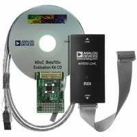
EVAL-ADUC7032QSPZ Analog Devices Inc, EVAL-ADUC7032QSPZ Datasheet - Page 7

EVAL-ADUC7032QSPZ
Manufacturer Part Number
EVAL-ADUC7032QSPZ
Description
EVAL DEV QUICK START ADUC7032
Manufacturer
Analog Devices Inc
Series
QuickStart™ PLUS Kitr
Type
MCUr
Datasheet
1.EVAL-ADUC7032QSPZ.pdf
(116 pages)
Specifications of EVAL-ADUC7032QSPZ
Contents
Evaluation Board, Power Supply, Cable, Software, Emulator and Documentation
For Use With/related Products
ADuC7032
Lead Free Status / RoHS Status
Lead free / RoHS Compliant
Parameter
PACKAGE THERMAL
POWER REQUIREMENTS
1
2
3
4
5
6
7
8
9
10
11
12
13
14
15
16
17
18
19
20
21
22
23
24
25
26
27
28
29
30
31
32
33
34
Not guaranteed by production test, but by design and/or characterization data at production release.
Valid for current ADC gain setting of PGA = 4 to 64.
These numbers include temperature drift.
Tested at gain range = 4; self-offset calibration removes this error.
Measured with an internal short after an initial offset calibration.
Measured with an internal short.
Includes internal reference temperature drift.
Factory calibrated at gain = 1.
System calibration at specific gain range removes the error at this gain range at that temperature.
Valid when used in conjunction with the ADCREF (the low power mode reference error) MMR.
Typical noise in low power modes is measured with chop enabled.
Voltage channel specifications include resistive attenuator input stage.
Includes an initial system calibration.
System calibration removes this error at that temperature.
RMS noise is referred to voltage attenuator input. For example, at f
ADC self-offset calibration removes this error.
Valid after an initial self-calibration.
Factory calibrated for the internal temperature sensor during final production test.
In ADC low power mode, the input range is fixed at ±9.375 mV. In ADC low power plus mode, the input range is fixed at ±2.34375 mV.
It is possible to extend the ADC input range by up to 10% by modifying the factory set value of the gain calibration register or using system calibration. This approach
Limited by minimum/maximum absolute input voltage range.
Valid for a differential input less than 10 mV.
Measured using box method.
The long-term stability specification is noncumulative. The drift in subsequent 1000 hour periods is significantly lower than in the first 1000 hour period.
References of up to REG_AVDD can be accommodated by enabling an internal divide-by-2.
Die temperature.
Endurance is qualified to 10,000 cycles, as per JEDEC Std. 22 Method A117, and measured at −40°C, +25°C, and +125°C. Typical endurance at 25°C is 170,000 cycles.
Retention lifetime equivalent at junction temperature (T
Low power oscillator can be calibrated against either the precision oscillator or the external 32.768 kHz crystal in user code.
These numbers are not production tested but are supported by LIN compliance testing.
The MCU core is not shut down, but an interrupt is generated, if enabled.
Thermal impedance can be used to calculate the thermal gradient from ambient to die temperature.
Typical additional supply current consumed during Flash/EE memory program and erase cycles is 7 mA and 5 mA, respectively.
yields these input referred noise figures.
can also be used to reduce the ADC input range (LSB size).
Internal regulated supply available at REG_DVDD (I
Power Supply Voltages
Power Consumption
SPECIFICATIONS
Thermal Shutdown
Thermal Impedance (θ
VDD (Battery Supply)
REG_DVDD, REG_AVDD
I
I
I
I
I
DD
DD
DD
DD
DD
(Precision Oscillator)
(MCU Normal Mode)
(MCU Powered Down)
(Current ADC)
ADC)
(Voltage/Temperature
31
JA
)
32
33
34
1
Test Conditions/Comments
48-lead LQFP, stacked die
Top die
Bottom die
MCU clock rate = 10.24 MHz, ADC off
MCU clock rate = 20.48 MHz, ADC off
ADC low power mode, measured over an ambient temperature range
of −10°C to +40°C (continuous ADC conversion)
ADC low power mode, measured over an ambient temperature range
of −40°C to +85°C (continuous ADC conversion)
ADC low power plus mode, measured over an ambient temperature
range of −10°C to +40°C (continuous ADC conversion)
Average current, measured with wake-up and watchdog timer
clocked from low power oscillator (−40°C to +85°C)
Average current, measured with wake-up and watchdog timer clocked
from low power oscillator over an ambient temperature range of −10°C
to +40°C
Per ADC
SOURCE
J
) = 85°C, as per JEDEC Std. 22 Method A117. Retention lifetime derates with junction temperature.
= 5 mA) and REG_AVDD (I
ADC
= 1 kHz, typical rms noise at the ADC input is 7.5 μV, which, when scaled by the attenuator (24),
Rev.0 | Page 7 of 116
SOURCE
= 1 mA).
Min
140
3.5
2.5
Typ
150
50
25
2.6
10
20
300
300
520
120
120
1.7
0.5
400
ADuC7032-8L
Max
160
18
2.7
20
30
400
500
700
300
175
mA
Unit
°C
°C/W
°C/W
V
V
mA
mA
μA
μA
μA
μA
μA
mA
μA


