CY8CKIT-001 Cypress Semiconductor Corp, CY8CKIT-001 Datasheet - Page 10
CY8CKIT-001
Manufacturer Part Number
CY8CKIT-001
Description
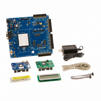
KIT DEV FOR PSOC3/5
Manufacturer
Cypress Semiconductor Corp
Series
PSoC® CapSenser
Type
MCUr
Datasheets
1.CY8CKIT-001.pdf
(2 pages)
2.CY8CKIT-001.pdf
(5 pages)
3.CY8CKIT-001.pdf
(116 pages)
4.CY8CKIT-001.pdf
(12 pages)
Specifications of CY8CKIT-001
Contents
Board, CD, CY8C29 & CY8C38 Modules, MiniProg3 Programmer/Debugger, Power Supply
Processor To Be Evaluated
CY8C29, CY8C38
Interface Type
RS-232, USB, JTAG
Operating Supply Voltage
3.3 V, 5 V
Lead Free Status / RoHS Status
Lead free / RoHS Compliant
For Use With/related Products
PSoC 1, PSoC 3 and PSoC 5
Lead Free Status / Rohs Status
Lead free / RoHS Compliant
Other names
428-2961
Available stocks
Company
Part Number
Manufacturer
Quantity
Price
Company:

Part Number:
CY8CKIT-001A
Manufacturer:
Cypress Semiconductor
Quantity:
135


Introduction
1.4
1.4.1
6
PSoC Development Board
The CY8CKIT-001 PSoC Development Board is designed to aid hardware, firmware, and software
developers in building their own systems around Cypress 8-bit and 32-bit PSoC devices. The
flexibility to configure the power domains is one of the foremost features of this board. Input power to
the board is from one of two sources:
■
■
This full featured board incorporates three onboard linear regulators that power peripherals and
PSoC modules at voltages between 1.72V and 5.5V. These regulators include a fixed 5V 1A linear
regulator, a fixed 3.3V 300 mA linear regulator, and a 1.5V to 5.5V 300 mA adjustable regulator. The
board also provides the ability to separate the PSoC core VCC rail into two separate rails, analog
and digital. In addition, the board is able to separate the I/O VCC rails, giving the flexibility to power
the I/O ports at different voltages.
The board is equipped with a 2x16 alphanumeric LCD module capable of 1.8V to 5.5V I/O. In addi-
tion, there is a mini-B full speed USB interface and a female DB9 serial communications interface.
Also included is a x-pin wireless radio module interface which can be used to develop CyFi™ Low-
Power RF or other embedded RF solutions with this kit. The board also has a prototyping area con-
taining a small bread board complete with I/O port sockets nearby, multipurpose LEDs, mechanical
push buttons, and a multipurpose variable resistor. In addition, three capacitive sensing elements
(two buttons and a five segment slider) are included on the board to allow evaluation of CapSense™
applications.
The board has four GPIO expansion slots, allowing the I/O to expand to external boards.
The board was designed with modularity in mind and, as a result, supports removable processor
modules. This allows you to plug different PSoC modules into the board based upon the desired fea-
tures of both 8-bit and 32-bit PSoC devices.
Default Switch and Jumper Settings
Jumpers on the CY8CKIT-001 PSoC Development Main Board have a default setting for 3.3V oper-
ation. For Default configuration, each of the jumpers must be set according to these instructions.
Note: All CY8C29x66 family processor module example projects are configured for 5V. Do configure
the board to 5V, before creating the example projects.
SW3 - VDD Select. Default Position: 3.3V (down position)
12V 1A wall wart power supply
9V alkaline battery (not included)
CY8CKIT-001 PSoC Development Kit Guide, Doc. # 001-48651 Rev. **
[+] Feedback
Related parts for CY8CKIT-001
Image
Part Number
Description
Manufacturer
Datasheet
Request
R

Part Number:
Description:
KIT DEV FOR PSOC3/5
Manufacturer:
Cypress Semiconductor Corp
Datasheet:

Part Number:
Description:
PSoC1/3/5 Development Kit
Manufacturer:
Cypress Semiconductor Corp
Datasheet:

Part Number:
Description:
KIT DEV PSOC PROC MODULE CY8C38
Manufacturer:
Cypress Semiconductor Corp

Part Number:
Description:
KIT DEV PSOC PROC MODULE CY8C29
Manufacturer:
Cypress Semiconductor Corp

Part Number:
Description:
KIT DEV PSOC ANALOG VOLTMETER
Manufacturer:
Cypress Semiconductor Corp
Datasheet:

Part Number:
Description:
KIT DEV PSOC5 FIRST TOUCH
Manufacturer:
Cypress Semiconductor Corp
Datasheet:

Part Number:
Description:
KIT DEV PSOC3 FIRSTTOUCH STARTER
Manufacturer:
Cypress Semiconductor Corp
Datasheet:
Part Number:
Description:
KIT DEV PROC MODULE PSOC5
Manufacturer:
Cypress Semiconductor Corp
Datasheet:

Part Number:
Description:
KIT PSOC CY8C28 FAMILY PROCESSOR
Manufacturer:
Cypress Semiconductor Corp
Datasheet:

Part Number:
Description:
KIT PSOC MINIPROG3 PROGRAM DEBUG
Manufacturer:
Cypress Semiconductor Corp
Datasheet:

Part Number:
Description:
KIT EVAL POWERLINE HIGH VOLT
Manufacturer:
Cypress Semiconductor Corp
Datasheet:

Part Number:
Description:
KIT PSOC FIRST TOUCH
Manufacturer:
Cypress Semiconductor Corp
Datasheet:

Part Number:
Description:
EVAL KIT WORLDTOUR2
Manufacturer:
Cypress Semiconductor Corp
Datasheet:

Part Number:
Description:
KIT UNIVERSAL CAPSENSE CTRLR
Manufacturer:
Cypress Semiconductor Corp
Datasheet:
