CY8CKIT-001 Cypress Semiconductor Corp, CY8CKIT-001 Datasheet - Page 110
CY8CKIT-001
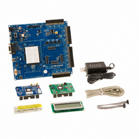
Manufacturer Part Number
CY8CKIT-001
Description
KIT DEV FOR PSOC3/5
Manufacturer
Cypress Semiconductor Corp
Series
PSoC® CapSenser
Type
MCUr
Datasheets
1.CY8CKIT-001.pdf
(2 pages)
2.CY8CKIT-001.pdf
(5 pages)
3.CY8CKIT-001.pdf
(116 pages)
4.CY8CKIT-001.pdf
(12 pages)
Specifications of CY8CKIT-001
Contents
Board, CD, CY8C29 & CY8C38 Modules, MiniProg3 Programmer/Debugger, Power Supply
Processor To Be Evaluated
CY8C29, CY8C38
Interface Type
RS-232, USB, JTAG
Operating Supply Voltage
3.3 V, 5 V
Lead Free Status / RoHS Status
Lead free / RoHS Compliant
For Use With/related Products
PSoC 1, PSoC 3 and PSoC 5
Lead Free Status / Rohs Status
Lead free / RoHS Compliant
Other names
428-2961
Available stocks
Company
Part Number
Manufacturer
Quantity
Price
Company:

Part Number:
CY8CKIT-001A
Manufacturer:
Cypress Semiconductor
Quantity:
135


Board Specifications and Layout
A.1.4.1
A.1.4.2
A.1.5
A.1.6
A.1.6.1
A.1.6.2
106
R31 - LCD Contrast Adjustment
The board is equipped with an LCD contrast adjustment resistor R31. Turning the wiper counter-
clockwise increases the contrast, while turning the wiper clockwise decreases the contrast.
J12 - LCD Module Power
Power for the LCD module is provided through header J12. Placing a jumper on the upper two pins
shorts the VCC pin of the module to ground. Placing the jumper on the lower two pins provides 5V to
the VCC pin of the module. This 5V power is taken directly from the onboard 5V regulator.
CapSense Elements
The prototyping area has three capacitive sensing elements. There are two CapSense buttons con-
nected directly to port zero pins. In addition, there is a five segment CapSense slider also connected
directly to port zero. Series resistors are placed on these port zero I/Os and should be loaded with
appropriate values. A value of 0Ω is used for general purpose CapSense applications, but a value of
560Ω should be used for achieving best performance. The board is loaded with 0Ω series resistors
by default. The presence of CapSense elements does not affect the general purpose use of port
zero pins.
Processor Module
J2, J3, J4 and J5 - VDDIO Select
These four headers allow the user to power the PSoC GPIOs at different voltages. For instance,
some of the I/O may be powered at 5V, some at 3.3V and some at 1.8V. There are four blocks of
GPIO, each having its own source power. Each VDDIO header provides power to specific GPIO's
and is selectable from VDD, 3.3V or VADJ. For details on which GPIOs are powered by which
VDDIO header, refer to the data sheet for the PSoC device used with this board.
For example, VDDIO_0 is configured to VDD, VDDIO_1 is configured to 3.3V and VDDIO_2 is con-
figured to VADJ by placing the jumpers in the respective positions as shown in
Figure A-7. VDDIO Select
SW4 - Processor Reset Button
The board has a push button switch that resets the PSoC device attached to the processor module.
One side of the switch is tied to the XRES pin of the processor module socket. The other end of the
switch is tied to the HW_RESET pin of the processor module socket. Doing this allows the module
VDDIO_0=VDD(5V/3.3V)
CY8CKIT-001 PSoC Development Kit Guide, Doc. # 001-48651 Rev. **
VDDIO_1=3.3V
VDDIO_2=VADJ
Figure
A-7.
[+] Feedback
Related parts for CY8CKIT-001
Image
Part Number
Description
Manufacturer
Datasheet
Request
R

Part Number:
Description:
KIT DEV FOR PSOC3/5
Manufacturer:
Cypress Semiconductor Corp
Datasheet:

Part Number:
Description:
PSoC1/3/5 Development Kit
Manufacturer:
Cypress Semiconductor Corp
Datasheet:

Part Number:
Description:
KIT DEV PSOC PROC MODULE CY8C38
Manufacturer:
Cypress Semiconductor Corp

Part Number:
Description:
KIT DEV PSOC PROC MODULE CY8C29
Manufacturer:
Cypress Semiconductor Corp

Part Number:
Description:
KIT DEV PSOC ANALOG VOLTMETER
Manufacturer:
Cypress Semiconductor Corp
Datasheet:

Part Number:
Description:
KIT DEV PSOC5 FIRST TOUCH
Manufacturer:
Cypress Semiconductor Corp
Datasheet:

Part Number:
Description:
KIT DEV PSOC3 FIRSTTOUCH STARTER
Manufacturer:
Cypress Semiconductor Corp
Datasheet:
Part Number:
Description:
KIT DEV PROC MODULE PSOC5
Manufacturer:
Cypress Semiconductor Corp
Datasheet:

Part Number:
Description:
KIT PSOC CY8C28 FAMILY PROCESSOR
Manufacturer:
Cypress Semiconductor Corp
Datasheet:

Part Number:
Description:
KIT PSOC MINIPROG3 PROGRAM DEBUG
Manufacturer:
Cypress Semiconductor Corp
Datasheet:

Part Number:
Description:
KIT EVAL POWERLINE HIGH VOLT
Manufacturer:
Cypress Semiconductor Corp
Datasheet:

Part Number:
Description:
KIT PSOC FIRST TOUCH
Manufacturer:
Cypress Semiconductor Corp
Datasheet:

Part Number:
Description:
EVAL KIT WORLDTOUR2
Manufacturer:
Cypress Semiconductor Corp
Datasheet:

Part Number:
Description:
KIT UNIVERSAL CAPSENSE CTRLR
Manufacturer:
Cypress Semiconductor Corp
Datasheet:
