CY8CKIT-001 Cypress Semiconductor Corp, CY8CKIT-001 Datasheet - Page 111
CY8CKIT-001
Manufacturer Part Number
CY8CKIT-001
Description
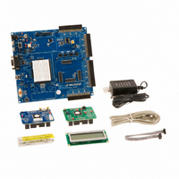
KIT DEV FOR PSOC3/5
Manufacturer
Cypress Semiconductor Corp
Series
PSoC® CapSenser
Type
MCUr
Datasheets
1.CY8CKIT-001.pdf
(2 pages)
2.CY8CKIT-001.pdf
(5 pages)
3.CY8CKIT-001.pdf
(116 pages)
4.CY8CKIT-001.pdf
(12 pages)
Specifications of CY8CKIT-001
Contents
Board, CD, CY8C29 & CY8C38 Modules, MiniProg3 Programmer/Debugger, Power Supply
Processor To Be Evaluated
CY8C29, CY8C38
Interface Type
RS-232, USB, JTAG
Operating Supply Voltage
3.3 V, 5 V
Lead Free Status / RoHS Status
Lead free / RoHS Compliant
For Use With/related Products
PSoC 1, PSoC 3 and PSoC 5
Lead Free Status / Rohs Status
Lead free / RoHS Compliant
Other names
428-2961
Available stocks
Company
Part Number
Manufacturer
Quantity
Price
Company:

Part Number:
CY8CKIT-001A
Manufacturer:
Cypress Semiconductor
Quantity:
135


A.1.6.3
A.1.6.4
CY8CKIT-001 PSoC Development Kit Guide, Doc. # 001-48651 Rev. **
designer to tie the HW_RESET line either high or low, depending on which direction the processor
reset is active.
Note PSoC1 devices are active high reset. Therefore, a light pull-down resistor may be necessary
on the XRES pin of designs with these devices to avoid unintentional device resets. PSoC3 and
PSoC5 devices are active low reset. Therefore, a light pull-up resistor may be necessary on the
XRES pin of designs with these devices to avoid unintentional device resets.
U8 - External MHz Oscillator
The board supports the use of an external high frequency 8-pin PDIP oscillator. The speed of the
oscillator supported is dependent on the specifications of the PSoC device used.
P1, P2, P3 and P4 - Processor Module Receptacles
Processor modules provide modularity to this board. Sockets P1-P4 are used to connect a processor
module to the board. All supported GPIOs (including special I/Os), along with VDD DIG, VDD ANLG,
5V, 3.3V, VBUS and VBAT (only connected to a surface mount pad on the board) are connected to
these receptacles. In addition, each of the VDDIO power pins are connected to these receptacles.
The full speed USB D+ and D- signals are also connected to one of the sockets. Processor reset is
connected to P1. Any “no connect” pins are brought out to surface mount test pads.
Figure A-8. Mechanical Layout Details for Processor Module Connector
Board Specifications and Layout
107
[+] Feedback
Related parts for CY8CKIT-001
Image
Part Number
Description
Manufacturer
Datasheet
Request
R

Part Number:
Description:
KIT DEV FOR PSOC3/5
Manufacturer:
Cypress Semiconductor Corp
Datasheet:

Part Number:
Description:
PSoC1/3/5 Development Kit
Manufacturer:
Cypress Semiconductor Corp
Datasheet:

Part Number:
Description:
KIT DEV PSOC PROC MODULE CY8C38
Manufacturer:
Cypress Semiconductor Corp

Part Number:
Description:
KIT DEV PSOC PROC MODULE CY8C29
Manufacturer:
Cypress Semiconductor Corp

Part Number:
Description:
KIT DEV PSOC ANALOG VOLTMETER
Manufacturer:
Cypress Semiconductor Corp
Datasheet:

Part Number:
Description:
KIT DEV PSOC5 FIRST TOUCH
Manufacturer:
Cypress Semiconductor Corp
Datasheet:

Part Number:
Description:
KIT DEV PSOC3 FIRSTTOUCH STARTER
Manufacturer:
Cypress Semiconductor Corp
Datasheet:
Part Number:
Description:
KIT DEV PROC MODULE PSOC5
Manufacturer:
Cypress Semiconductor Corp
Datasheet:

Part Number:
Description:
KIT PSOC CY8C28 FAMILY PROCESSOR
Manufacturer:
Cypress Semiconductor Corp
Datasheet:

Part Number:
Description:
KIT PSOC MINIPROG3 PROGRAM DEBUG
Manufacturer:
Cypress Semiconductor Corp
Datasheet:

Part Number:
Description:
KIT EVAL POWERLINE HIGH VOLT
Manufacturer:
Cypress Semiconductor Corp
Datasheet:

Part Number:
Description:
KIT PSOC FIRST TOUCH
Manufacturer:
Cypress Semiconductor Corp
Datasheet:

Part Number:
Description:
EVAL KIT WORLDTOUR2
Manufacturer:
Cypress Semiconductor Corp
Datasheet:

Part Number:
Description:
KIT UNIVERSAL CAPSENSE CTRLR
Manufacturer:
Cypress Semiconductor Corp
Datasheet:
